Physical and Electrical Properties of Defects Formed in Rapid Thermal Processing
- PDF / 2,802,364 Bytes
- 12 Pages / 414.72 x 648 pts Page_size
- 54 Downloads / 366 Views
ABSTRACT RTP will be replaced with some of the conventional thermal processing employed in ULSI fabrication lines in near future. We show at first the device characteristics demanded for next generation DRAM which is a typical example of ULSIs and some issues to satisfy the demands. Next we show some candidates for RTP in the ULSI processes and discuss difference between RTP and the conventional thermal processes. We think one of the largest difference is the quenching Si wafers after short time annealing and by the quenching the deep levels due to fast diffusing atoms and point defects in Si are introduced. Experimental results of N2 and Cu related deep levels are shown as the examples of the deep levels induced by the quenching in Si. Finally, we propose the gettering method for them in RTP.
INTRODUCTION Rapid Thermal Processing (RTP) is necessary for the reduction of thermal budget demanded in near future ULSI fabrication processes. Many kinds of RTP equipments have been developed and some of them are now employed in ULSI processing. But some problems must be
overcome for RTP to be widely accepted in ULSI fabrication lines. Major problems are power efficiency of lamp heating RTP and throughput of resistive heating RTP equipments, and in terms of the ULSI process quality are precise control of temperatures and homogeneity of temperature distribution in a large processed wafer and impurity contamination and so on. The problems concerning to the above process quality will be expected to be overcome in near future. RTP must be replaced with some of the conventional thermal processing employed in ULSI fabrication lines. Therefore, at that time the RTP must be better than the conventional
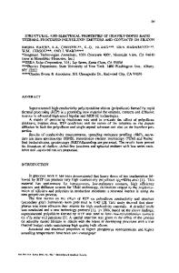
thermal processing in the whole (Fig.1). The ability such as cleanness and controllability of the conventional thermal processing advances day Dy day, because many kinds of demands are proposed from next generation ULSI. In this paper, at first we show the device characteristics demanded for next generation DRAM which is a typical example of ULSIs and second we show some issues to satisfy the demands. Third, some candidates for RTP in ULSI processes and fundamental difference between RTP and the conventional thermal processes will be shown. We think the difference is short time annealing and quenching of Si wafers. Fourth, we show experimental results of the deep levels which are induced by the quenching, that is N2 and Cu related deep levels in Si. Finally, we show some aspects about the RTP in conclusion.
275
Mat. Res. Soc. Symp. Proc. Vol. 470 01997 Materials Research Society
p"/p+ epitaxialwafer
a V
tJ 0
a 0
iM
4M
16M
64M
256M
IG
Fig. 1. Cleanness and quality of Si crystal demanded for thermal processing vs. DRAM generation
ance plate
iM
4M 16M 64M DRAM Bit Capacity (bit)
256M
Fig.3. DRAM leakage paths, path 1: leakage to a substrate via pn junction, path2: leakage to a cell plate via a capacitance insulation film, path 3:leakage to the bit line via a cell transistor, path 4:leakage between devices.
Fig.2.
Data Loading...