Physical characterization of HfO 2 deposited on Ge substrates by MOCVD
- PDF / 421,991 Bytes
- 6 Pages / 595 x 842 pts (A4) Page_size
- 83 Downloads / 281 Views
B5.4.1/D5.4.1
Physical characterization of HfO2 deposited on Ge substrates by MOCVD S. Van Elshocht, B. Brijs, M. Caymax, T. Conard, S. De Gendt, S. Kubicek, M. Meuris, B. Onsia, O. Richard, I. Teerlinck, J. Van Steenbergen, C. Zhao, and M. Heyns. IMEC vzw, Kapeldreef 75 B-3001 Heverlee (Leuven), Belgium
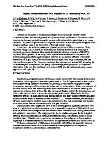
ABSTRACT Germanium is because of its intrinsically higher mobility than Si, currently under consideration as an alternative approach to improve transistor performance. Germanium oxide, however, is thermodynamically unstable, preventing formation of the gate dielectric by simple oxidation. At present, high-k dielectrics might be considered as an enabling technology as much progress has been made in the deposition of thin high-quality layers. In this paper, we study the growth and physical properties of HfO2 deposited on Ge by MOCVD, using TDEAH and O2 as precursors, and compare the results to similar layers deposited on silicon substrates. Our results show that the physical properties of MOCVDdeposited HfO2 layers on Ge are very similar to what we have observed in the past for Si. Unfortunately, some of the negative aspects observed for Si, such as diffusion of substrate material in the high-k layer, a low density for thinner layers, or a rough top surface, are also observed for the case of Ge. However, careful surface pretreatments such as NH3 annealing the Ge substrate prior to deposition, can greatly improve the physical properties. An important observation is the very thin interfacial layer between HfO2 and Ge substrate, allowing a more aggressive scaling for Ge. INTRODUCTION Traditionally, a higher transistor performance can be achieved by downscaling the transistor dimensions, including the thickness of the gate dielectric. The SiO2 gate dielectric is at present rapidly approaching a physical thickness limit, resulting in unacceptably high gate leakage currents thus leaving insufficient room for further scaling. Alternatively, further improvement of the drive current could also be accomplished by an enhancement of the channel mobility, for example by replacing Si by SiGe or Ge. The intrinsically higher mobility for both electrons and holes in Germanium results in an enhanced transistor performance. Historically, the first transistors were all Ge based, but the low thermal stability and water solubility of the GeO2 gate dielectric caused people to abandon Ge and switch to Si [1]. On the other hand, the last couple of years, much progress has been made in the deposition of thin high-quality high-k layers that could now form a feasible alternative for GeO2 as gate dielectric. Implementation of Ge might also prove to be an advantage from a gate stack point of view since it might solve some of the issues that prevent successful integration of HfO2 with Si, such there are, severe mobility degradation and formation of an interfacial layer limiting performance and scalability, respectively. The higher mobility for Ge might compensate for the degraded mobility while the lower stability of GeO2 is expected to result in
Data Loading...