Physical Vapor Deposition of Cu(In,Ga)Se 2 Films for Industrial Application
- PDF / 293,648 Bytes
- 12 Pages / 596 x 842 pts (A4) Page_size
- 102 Downloads / 259 Views
Physical Vapor Deposition of Cu(In,Ga)Se 2 Films for Industrial Application T. Wada1 , S. Nishiwaki, Y. Hashimoto and T. Negami Advanced Technology Research Laboratories, Matsushita Electric Ind. Co., Ltd., 3-4 Hikaridai, Seika-cho, Soraku-gun, Kyoto 619-0237, Japan 1 Department of Materials Chemistry, Ryukoku University, Seta, Otsu 520-2194, Japan ABSTRACT Cu(In,Ga)Se2 thin films were prepared by physical vapor deposition. The CIGS films were deposited by three kinds of method. The 1st was "2 -stage process" in which (In,Ga)2 Se3 precursor layer was deposited on Mo coated soda-lime glass at the 1st stage, and then exposed to Cu and Se fluxes to form CIGS films at the 2nd stage. The 2nd method was an ordinary "3-stage process". The 3rd method was “2-stage deposition and post-annealing process” in which CIGS films were deposited at low substrate temperatures and then the obtained CIGS precursor films were annealed in Se flux at high temperatures. A solar cell using a CIGS film prepared at 400 o C by the “2-stage process” showed an efficiency of 11.8 % and that using a CIGS film deposited at 350 o C by the “3-stage process” showed an efficiency of 12.4 %. The CIGS films deposited by the “2-stage deposition and post-annealing process” have similar microstructures to the device quality CIGS films deposited by the “3-stage process” at high temperatures. The solar cell with an MgF 2 /ITO/ZnO/CdS/CIGS/Mo/glass structure showed an efficiency of 17.5 % (Voc=0.634 V, Jsc=36.4 mA/cm2 , FF=0.756). The thin CIGS films with a smooth and flat surface can be fabricated by the “2-stage deposition and post-annealing process”. The solar cell using a 0.7µm CIGS absorber layer showed an efficiency of over 12 % and a large open circuit voltage of 0.677 V. INTRODUCTION Cu(In,Ga)Se2 (CIGS) has received considerable attention as one of the most promising materials for thin film solar cells. Recently, NREL and Matsushita have demonstrated efficienc ies of over 18 % for CIGS solar cells [1, 2]. Their CIGS films were deposited by “3-stage” process. In our previous paper [3, 4], we investigated grain growth and phase changes in the deposition of CIGS films under (In,Ga)-rich condition corresponding to the 2nd stage of the “3-stage” process. In the work, device quality CIGS films were prepared by “2-stage process” without the deposition of In-Ga-Se at the 3rd stage. The fabricated CIGS solar cell showed an efficiency of 16.6 %. In the next step of our study, we intend to prepare device quality CIGS films at low substrate temperatures. Deposition of CIGS films at low substrate temperatures has practical importance for not only reducing energy usage and lowering production costs for CIGS photovoltaic modules but also would allow flexibility in utilizing alternative substrate materials, such as flexible polymer films. In this work, CIGS films were prepared by three kinds of deposition method. The 1st H2.1.1
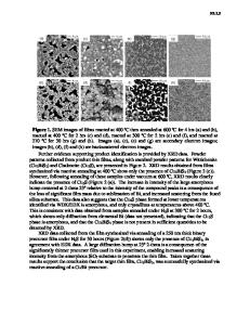
Constant IR Irradiation Thermocouple
Glass Mo Recorder
CIGS
Radiation
Fig. 1 Schematic diagram of the substrate temperature control and m
Data Loading...