Properties of the Interface between Amorphous Silicon and Nitride
- PDF / 2,468,176 Bytes
- 9 Pages / 417.6 x 639 pts Page_size
- 69 Downloads / 409 Views
PROPERTIES OF THE INTERFACE BETWEEN AMORPHOUS SILICON AND NITRIDE
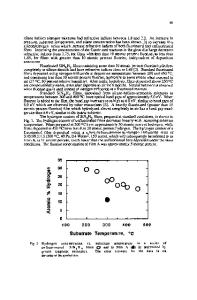
C. C. TSAI, R. A. STREET, F. A. PONCE and G. B. ANDERSON Xerox PARC, 3333 Coyote Hill Road, Palo Alto, CA 94304. ABSTRACT The structural, compositional and electronic properties of the a-Si:H/a-SiNx:h interface are reported. High resolution TEM and light/dark ESR studies conclude that the interface has a finite width of the order of 10 A. In addition, there is a high density of charges residing near the interface. Band bendings occur in both a-Si:H and a-SiNx:H, resulting in few neutral dangling bonds in the a-Si:H/a-SiNx:H multilayer structure. The depletion width in the nitride is of the order of 100 A. The slow decay of the LESR in multilayers with thin sublayers is attributed to charges trapped in the slow states in the nitride. INTRODUCTION Interfaces between hydrogenated amorphous silicon (a-Si:H) and silicon nitride (a-SiN,:H) are of importance in amorphous semiconductor superlattices [1,2] and thin film transistors [3,41. For most thin film semiconductor devices, interfaces play an influential role on their characteristics. The amorphous silicon TFTs are no exception where a-SiNx:H is used both as a gate dielectric and a passivation insulator. In amorphous semiconductor superlattices, quantum size effects are observed only in sublayers thinner than - 40 A, because the wavefunctions are more localized in amorphous semiconductors. Interface effects dominate since there can be as many as over a thousand interfaces in a film of 1 p•m in thickness. In addition, if interfaces have finite widths rather than being atomically abrupt, an increasing portion of the sample is made up of interface regions as the sublayers become thinner. When the sublayer thickness becomes comparable to the interface width, the entire sample contains only interfaces. Properties of the a-Si:H/a-SiN,:H interfaces are not well understood. Many questions remain. The two main issues are (1) the structure and compositional profile of the interface, and (2) the electronic states near the interface. For the former, it is not known whether an interface between two amorphous materials which lack long range order can be as abrupt as that formed between two crystals. Since both materials are prepared by plasma deposition, it is not clear if the highly reactive plasma can yield interfaces as abrupt as a more inert technique such as MBE or MOCVD. If interfaces have finite widths, then information on the width of the interface region is needed. Also the effect of the substrate roughness must be assessed along with the question whether the width and smoothness of the interface vary as the film growth progresses. In addition, both compositional and structural aspects must be considered regarding the sharpness of an interface. Since NH3 used for growing a-SiN,:H is known to linger in the reactor system causing cross contamination of the subsequently deposited bulk a-Si:H [5], it is of interest to compare the interface where a-SiN,:H is grown on a-Si:H (top nitride) and vice versa (bottom n
Data Loading...