Rapid Thermal Annealed Undoped LPCVD Si/Single Crystal Si Substrate Structures with an Implant of Si Near Interfaces
- PDF / 2,037,462 Bytes
- 6 Pages / 420.48 x 639 pts Page_size
- 28 Downloads / 294 Views
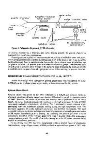
RAPID THERMAL ANNEALED UNDOPED LPCVD Si/SINGLE CRYSTAL Si SUBSTRATE STRUCTURES WITH AN IMPLANT OF Si NEAR INTERFACES S.Ogawa*, S.Okuda*, T.Kouzaki**, T.Yoshida*, and Y.Yoshioka** *Matsushita Electric, Semiconductor Research Center, Moriguchi, Osaka, Japan **Matsushita Technoresearch, Moriguchi, Osaka, Japan ABSTRACT The breaking up of a native oxide layer of a LPCVD amorphous Si/single crystal n+Si substrate interface by a rapid-thermal annealing was studied from movement and morphological change. Oxygen atoms the point of view of oxygen began to move at 1025 0C. After annealing at 1115 0C for 30sec, the quantity of oxygen atoms near the interface decreased dramatically and a silicon implant near the interface could enhance the decrease. More detailed observation was transmission electron carried out by cross-section high-resolution microscopy. After annealing at g40 °C for 30sec, the native oxide layer was continuous. On the qther hand, with a silicon implant near the interface, it changed into small oxide balls and an epitaxial growth occurred in the LPCVD layer with twins caused by these oxide balls. After annealing at 1115°C for 30sec, even without the silicon implant, a complete epitaxial growth occurred but it seemed that some SiOx particles dissolved into a single crystal Si layer near the interface. INTRODUCTION Great interest has been generated in the highly doped poly Si/single crystal Si substrate interface which strongly affects the electrical characteristics of semiconductor devices, especially in sub-pm-sized devices. Poly Si films are used in advanced integrated circuit technology as a diffusion source, simultaneously as an emitter contact and as an interconnect. Many studies have been focused on the interfacial layers and the crystallinity of Si films 11-4]. Bravman et al. have demonstrated that a morphological change of the poly Si/Si single crystal substrate interface has been correlated to the surface treatment used prior to poly Si deposition and to high-temperature annealing using a high-resolution transmission electron microscopy (HRTEM)[51, but annealing temperature was above 1000C, which is rather high for future sub-pm integrated circuit fabrication. In this paper, we show that a rapid thermal annealing (RTA) with an implant of silicon near the interface can break up the interfacial native oxide layer at a temperature lower than 1000C and also discuss on a morphological change of the native oxide layer after the RTA employing HRTEM. EXPERIMENTAL PROCEDURE Undoped 90nm-thick amorphous Si films were deposited on arsenic-doped single n+Si crystal wafers by a LPCVD method. Just prior to loading into a LPCVD reactor at a room temperature, silicon wafers, (100) in orientation, in 50:1 H20:HF. After loading wafers, the were chemically cleaned by an etch reactor was pumped down to lx10- 2 Torr and then heated up to a deposition5 2 temperature of 550°C. Some samples were followed by an implant of 3x101 /cm all samples were rapid thermal annealed in argon silicon at 65keV and finally atmosphere at 94
Data Loading...