Room Temperature Growth of Silicon Dioxide Using a Low Energy Ion Beam
- PDF / 343,453 Bytes
- 6 Pages / 420.48 x 639 pts Page_size
- 32 Downloads / 314 Views
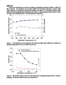
ROOM TEMPERATURE GROWTH OF SILICON DIOXIDE USING A LOW ENERGY ION BEAM S.S. TODOROV AND E.R. FOSSUM Department of Electrical Engineering and Columbia Radiation Laboratory, Columbia University, New York, NY 10027 ABSTRACT Ultra-thin films of silicon dioxide are formed on silicon surfaces at room temperature by direct bombardment with an oxygen-containing ion beam at energies of 150 eV or less. The process of film growth is studied.through ellipsometric measurements of their properties as a function of ion energy and dose, oxygen partial pressure and substrate temperature. Typical oxide thicknesses of the order of 50 A are obtained by three minute or longer exposures to beams of current density 135 4A/cm2 . Ion-beam grown oxides are compared to conventional thin oxide films grown at elevated temperatures and show the same stoichiometry. The growth rate decreases rapidly after a continuous oxide film has been formed. Performing the ion bombardment at elevated substrate temperatures leads to only small enhancement of the oxide growth indicating non-thermally driven reaction kinetics. INTRODUCTION Reduced-temperature oxidation of silicon has been demonstrated recently by a number of groups using a variety of methods. Among these are microwave plasma oxidation [1,2], photo-enhanced oxidation [3,4], remote plasma-enhanced chemical vapor deposition (CVD) [5], ion-beam oxidation [6,7] and, more recently [8]. We have previously reported the possibility of obtaining ultra-thin films of Si0 2 at room temperature by subjecting silicon wafers to bombardment by low energy oxygen ions [9]. The high electrical quality of the obtained oxide films has been demonstrated by their successful application as gate dielectrics in MOS transistors. It was noted that the films exhibited very good thickness uniformity over the area of 5-cm diameter wafers, characteristic of a self-limiting growth behavior. This paper presents the results of experiments performed to understand the growth mechanism of the films. EXPERIMENTAL DETAILS Thin silicon dioxide films are grown on device grade polished (100) silicon wafers of diameter 5 cm. The substrates are prepared by cleaning in wet chemical baths and by growing and stripping two successive thick oxide layers grown in steam at 900 0 C. The oxide growth i5 performed in a vacuum chamber with a base pressure of 2x10- torr by bombarding the samples with an ion beam produced by a 2.5-cm diameter single-grid Kaufman type ion source. The source operates on an argon-oxygen mixture with a total working pressure of 4 4x10torr. The samples are mounted on a substrate holder which allows the monitoring of the ion current density at the Mat. Res. Soc. Symp. Proc. Vol. 75. '1987 Materials Research Society
350
position of the substrate by swinging an ion probe into the beam. Following ion bombardment the samples are taken out of the vacuum chamber and the properties of the grown films are measured immediately on a Gaertner L117 ellipsometer operating at wavelength X = 6328 X and angle of incidence Gi = 700. The sa
Data Loading...