Strain Measurement and Calculation in Passivated Cu Lines Deposited by Three Different Methods
- PDF / 314,769 Bytes
- 6 Pages / 414.72 x 648 pts Page_size
- 72 Downloads / 299 Views
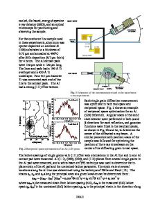
deposition techniques were used: sputter-reflow in a ultra-high vacuum (UHV) system, chemical vapor deposition (CVD), and electroplating. The wafers were a dense array of 1.0 jim width lines separated by 1.0 jim spaces. Stress was calculated from x-ray strain measurements made in the Generalized Focusing Diffractometer (GFD) housed at Stanford University. Standard sin 2y techniques were used [1]. Blanket films from each type of deposition were also measured to find texture and the unstressed lattice parameter. While these films were not put through a passivation step, they were UHV vacuum annealed to the same temperatures and times that the passivated lines saw. Texture scans were also made using the GFD to compare the three samples producing a 2-D slice of the pole plot. The {331 } reflections were used for the Cu samples [1]. The ANSYS finite element program was used to model these same structures [2]. RESULTS Texture Measurements Intensity vs. at (the complement of T) curves from the UHV film is shown in Figure 1. In
an ideal, unstressed Cu system we would expect to see intensity peaks at 22.00 and 48.50 in a for 639 Mat. Res. Soc. Symp. Proc. Vol. 403 ©1996 Materials Research Society
the {331 -type reflections for {1111 texture. The width of these peaks is a good indication of the amount of texturing in the films. We can see in Figure 1 that the reflow UHV copper had a very strong {1111 texture with a full width half maximum (FWHM) of the higher cc peak of 2.35'. The CVD Cu has no texture. The corresponding curve for that system has a highest intensity of 5.0 and has no peaks. The electroplated Cu showed very good {1111 texturing as well, looking much like the graph in Figure 1, with a FWHM of 2.4'. While no systematic study of the electromigration lifetimes of Cu as a function of strength of {1111 texture have been performed, it is reasonable to assume that the same correlation between strong texture and long electromigration lifetime seen for Al should be expected since voids should still try to form with low energy {1111 plane faces.
0 ;
100-
9080
70 60 50 40 30 20 10
0
I
0
L
10
-
I
20
I
t
I
30 40 Alpha Figure 1: Intensity vs. ox curve for reflow Cu showing 1111} texture
i I
I
50
60
Stress Measurements Blanket film measurements of stress in the Cu films are presented in Table 1. There are differences in stress levels for the three blanket films. The CVD processing temperature, which was 175 0 C, accounts for the lower stress value than that seen in the UHV Cu, deposited at room temperature, but reflowed at 400'C. The stress in the electroplated Cu can be attributed to intrinsic stress during deposition. Another factor in these measurements may be the effect of texture of the films and the number of {3311 planes that are reflecting at a given cc. The blanket film stresses are biaxial in the plane of the film, relatively low, and slightly higher than typically seen for Al-Cu films at room temperature (about 180 MPa) [3]. Stresses in passivated copper 1 jim lines are about the same for b
Data Loading...