Stress Mapping of SiC Wafers by Synchrotron White Beam X-ray Reticulography
- PDF / 1,446,091 Bytes
- 6 Pages / 612 x 792 pts (letter) Page_size
- 29 Downloads / 244 Views
1069-D07-07
Stress Mapping of SiC Wafers by Synchrotron White Beam X-ray Reticulography Ning Zhang1, Yi Chen1, Edward Sanchez2, Michael F MacMillan2, and Michael Dudley1 1 Department of Materials Science and Engineering, Stony Brook University, Stony Brook, NY, 11794-2275 2 Dow Corning Compound Semiconductor Solutions, Midland, MI, 48611 ABSTRACT Synchrotron white beam x-ray reticulography has been used to quantitatively map the residual stress/strain in SiC wafers. The basic principle of our study is that there exists a relationship between the stress state in a crystal and the local lattice plane orientation and that this relationship can be exploited in order to determine the full strain tensor as a function of position inside the crystal. The theoretical background involved in stress mapping using synchrotron white beam x-ray reticulography is introduced based on the change of the normal to a lattice plane due to the distortion associated with the residual strain. The stress in a region of a commercial 4H silicon carbide wafer has been studied using this technique and the results are discussed. This technique can in principle be used in any single crystal material. INTRODUCTION Silicon carbide (SiC) is well known as a potential semiconductor material for applications under extreme circumstances due to its outstanding properties such as high thermal conductivity, high breakdown voltage and high saturated electron drift velocity [1]. Accurate measurement of the residual stress/strain in as-grown SiC wafers is of great interest because measured values can allow validation of the thermal stress calculations used to design optimal crystal growth parameters. This is of particular importance in SiC since thermal stresses lead to the activation of basal plane slip systems resulting in significant densities of basal plane dislocations which are implicated in the forward voltage drop under forward bias in pin diodes. Other techniques that can be used to measure stress distributions in SiC crystals include high-resolution x-ray diffraction and Raman spectroscopy. However, mapping the full strain/stress tensor using these techniques can be extremely time-consuming. Here we identify a technique which can be used to map the complete strain/stress state of a large-area SiC wafer in a fast, effective and accurate way. This technique is based on the application of the ray-tracing principle to x-ray reticulography [2]. EXPERIMENT A 20 mm x 27 mm area in a 3 in. 4H-SiC wafer was studied. A fine scale x-ray absorbing mesh with periodicity of 1 mm placed on the x-ray exit surface of the sample splits the diffracted beams into an array of microbeams. The imaging was carried out at the Stony Brook Synchrotron Topography Station (Beamline X-19C) at Brookhaven National Laboratory using Agfa Structurix D3-SC film at a specimen-film distance of 10 - 15 cm for transmission geometry.
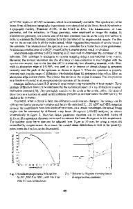
Figure 1. Schematic diagram showing the geometry used in the reticulography. (x0, y0), (x1, y1), (x2, y2) and (x3, y3) are the coordinates of the spots on t
Data Loading...


