Structural and Electronic Properties of Negative Electron Affinity Epitaxial Diamond (110) Films Studied Using Atomic Re
- PDF / 2,600,130 Bytes
- 6 Pages / 414.72 x 648 pts Page_size
- 48 Downloads / 293 Views
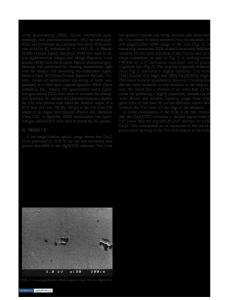
ABSTRACT We report ultrahigh vacuum (UHV) scanning tunneling microscopy (STM) studies of the structural and electronic properties of epitaxial diamond (110) films. We observe that epitaxial diamond (110) films grow very rough due to striations. The striations are found to be due to the appearance of(1 11) faces and contain (100) steps. UHV STM atomic resolution images of the diamond (110) films show a (lxi) zigzag structure that measures 1.5 + 0.1 A x 1.5 + 0.1 A, in agreement with theoretical predictions for the hydrogen terminated diamond (110) surface. Ultraviolet spectroscopy shows that the epitaxial films have a photoelectric threshold of 5.3 ± 0.1 eV, providing evidence that the films have a negative electron affinity surface. INTRODUCTION The diamond (110) surface is reported to grow the fastest among the low index planes and very rough [1]. In addition, the hydrogen terminated surface has been reported to have a negative electron affinity (NEA) [2]. However, the atomic structure of the diamond (110) surface and its relation to surface electronic properties are not well understood. In order to study the diamond (110) surface, epitaxial diamond (110) films are grown on synthetic (110) diamond substrates using chemical vapor deposition (CVD). The CVD grown diamond films are transferred to an ultrahigh vacuum (UHV) system without exposing them to air, and studied using UHV scanning tunneling microscopy (STM). We observe that epitaxial diamond (110) films have a very rough surface, in contrast to epitaxial diamond (100) and (111) films. We find that striation is the dominant morphology on the diamond (110) surface. The striations are due to the appearance of the (111) face and contain (100) steps. We report, for the first time, atomic resolution images of the (lxi) diamond (110) surface using UHV STM. The lxi unit cell measures 1.5 ± 0.1 A x 1.5 ± 0.1 A, in agreement with theoretical predictions for the hydrogen terminated diamond (110) surface [3]. Ultraviolet spectroscopy shows that the (110) epitaxial films have a photoelectric threshold of 5.3 ± 0.1 eV, providing evidence that the films have an NEA surface. However, it is known that hydrogen terminated diamond (100) and (111) surfaces have NEA [2]. Therefore, since the (110) epitaxial films contain (111) faces and (100) steps, the NEA of the epitaxial (110) films may be due to these faces and steps, and it is not possible to conclude that the (110) surface has NEA. EXPERIMENT The epitaxial diamond films are grown on 2.0 x 2.0 x 0.25 mm 3 synthetic type II b diamond (110) substrates obtained from Harris Corporation. The diamond substrate is cleaned ultrasonically with acetone and methanol, and in an HNO 3 :HCL (1:3) mixture at room temperature for 30 minutes. The substrate is then rinsed in de-ionized water and mounted on a 165 Mat. Res. Soc. Symp. Proc. Vol. 509 ©1998 Materials Research Society
quartz plate using a Mo holder. The epitaxial film is grown using a hot-tungsten-filamentassisted CVD reactor. The reactor is coupled to the UHV STM chamber via an
Data Loading...