Structure Analysis of CeO 2 /ZrO 2 /Si Multilayer Thin Films by Hrtem
- PDF / 2,010,329 Bytes
- 6 Pages / 415.8 x 637.2 pts Page_size
- 102 Downloads / 423 Views
improve the matching between the film and the substrate, to prevent the reaction between them, and so on. It is well known that oxides that can be grown epitaxially on Si(001) substrates are limited to certain kinds of materials [1,2]. CeO2 is one of the most attractive materials due to its high chemical stability, relatively high dielectric constant (cr=26 [3]), and the very small lattice mismatch between CeO2(l00) and Si(100) (-0.36% at room temperature). Therefore, it is expected that CeO 2 thin films will grow epitaxially on Si(001) with (001) orientation. However it has been reported that CeO 2 thin films do not exibit (001) orientation, but (110) and/or (111) orientation on Si(001) substrates [3,4,5,6], which indicates that it is difficult to obtain heteroepitaxially grown CeO2 on Si(001) with cube-on-cube relations. On the other hand, CeO2/YSZ/Si(001) has all heteroepitaxial structure with cube-on-cube relations at both the CeO,/YSZ and the YSZ/Si interfaces. Because of this, the CeO 2/YSZ double buffer layer structure is widely used to realize heteroepitaxial growth of several oxides having perovskite structure such as YBa 2Cu 307., [7] and SrTiO 3 [8] on Si(001). YSZ (8 mol% Y203) has cubic fluorite structure and good oxygen conductivity. It is known that the oxygen vacancy in YSZ causes "ion drift", therefore epitaxial YSZ/Si thin films have undesirable C-V characteristic [9]. On the other hand, it is also reported that CeO 2/Si thin films do not show such 183
Mat. Res. Soc. Symp. Proc. Vol. 592 © 2000 Materials Research Society
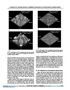
"ion drift" [10]. Consequently, a CeO2/YSZ/Si(001) structure with an ultra thin YSZ buffer layer is required. According to previous work [8], the heteroepitaxial growth of CeO2 occurs with 3 nmu thick YSZ thin films. Moreover, in our study, it is confirmed that even 0.5 nun of YSZ has an effect on the cube-on-cube epitaxial CeO 2 growth according to XRD [11]. However, it has not known how the nanostructure of these multilayer films and the interfaces change depending on the YSZ thickness. The purpose of this work is to clarify the effect of the YSZ thickness on the nanostructure of CeO 2 /YSZ multilayer thin films by HRTEM analysis. EXPERIMENT YSZ and CeO2 thin films were deposited by pulsed laser deposition (PLD) with a KrF excimer
laser (4=248 nm). The laser beam energy density was about 1.0 J/cm 2. Si(001) substrates were cleaned by the RCA and HF process to remove any SiOx surface layer just before the deposition. Then the substrate was immediately put into the processing chamber. In this experiment, substrates were heated to 800 'C at 5 x 10' Torr. YSZ deposition was started at this pressure without the introduction of 02 gas. 30 sec after laser pulsing began, 02 gas was introduced to 5.5 x 10' Torr. The detailed conditions of the deposition of the CeO 2/YSZ/Si thin films have been previously reported [12]. Cross sectional specimens for TEM analysis were prepared by bonding and conventional ionpolshing methods (PIPS model 691, Gatan, U.S.A.) The atomic structures were obs
Data Loading...