Structure characterization of MHEMT heterostructure elements with In 0.4 Ga 0.6 As quantum well grown by molecular beam
- PDF / 684,313 Bytes
- 5 Pages / 612 x 792 pts (letter) Page_size
- 1 Downloads / 275 Views
MATERIALS
Structure Characterization of MHEMT Heterostructure Elements with In0.4Ga0.6As Quantum Well Grown by Molecular Beam Epitaxy on GaAs Substrate Using Reciprocal Space Mapping A. N. Aleshina, A. S. Bugaeva, M. A. Ermakovab, and O. A. Rubana a
Institute of Ultra High Frequency Semiconductor Electronics, Russian Academy of Sciences, Moscow, 117105 Russia b Center for Study of Surface and Vacuum Properties, Federal Agency on Technical Regulating and Metrology, Moscow, 119421 Russia e-mail: [email protected] Received May 7, 2015
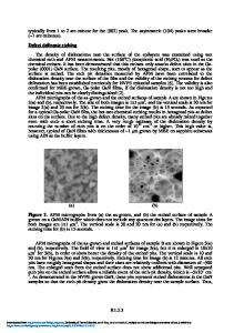
Abstract—The crystallographic parameters of elements of a metamorphic high-electron-mobility transistor (MHEMT) heterostructure with In0.4Ga0.6As quantum well are determined using reciprocal space mapping. The heterostructure has been grown by molecular-beam epitaxy (MBE) on the vicinal surface of a GaAs substrate with a deviation angle of 2° from the (001) plane. The structure consists of a metamorphic step-graded buffer (composed of six layers, including an inverse step), a high-temperature buffer of constant composition, and active high-electron-mobility transistor (HEMT) layers. The InAs content in the metamorphic buffer layers varies from 0.1 to 0.48. Reciprocal space mapping has been performed for the 004 and 224 reflections (the latter in glancing exit geometry). Based on map processing, the lateral and vertical lattice parameters of InxGa1 – xAs ternary solid solutions of variable composition have been determined. The degree of layer lattice relaxation and the compressive stress are found within the linear elasticity theory. The high-temperature buffer layer of constant composition (on which active MHEMT layers are directly formed) is shown to have the highest (close to 100%) degree of relaxation in comparison with all other heterostructure layers and a minimum compressive stress. DOI: 10.1134/S1063774516020036
INTRODUCTION Heterostructures based on InGaAs/InAlAs ternary solid solutions are widely used in microwave electronics and optoelectronics. Heterostructures with an indium content of 40 at % in the transistor channel are generally grown on GaAs substrates in view of their technological advantages. An increase in the molar fraction of indium in InGaAs/InAlAs ternary solutions leads to a rapid increase in the layer lattice parameter and, correspondingly, in the lattice mismatch with the GaAs substrate. These structures can be only grown using a metamorphic buffer. The concept of metamorphic buffer implies the growth of a transition layer between the substrate and the active transistor layer (with a composition of InAlAs ternary solid solution gradually changing with depth) [1–4]. The active part of the device (quantum well (QW)) must be unstrained. In addition, it must be free of threading dislocations that form as a result of lateral lattice mismatch between adjacent layers. Metamorphic buffers may have different designs: a step-graded buffer or a buffer with a linear change in indium concentration. The design should provide the absence of stress in the active layers; it
Data Loading...