Study of Electrical Properties of Dislocations in ZNS Using Electric Force Microscopy
- PDF / 2,525,515 Bytes
- 6 Pages / 417.6 x 639 pts Page_size
- 87 Downloads / 267 Views
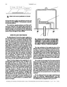
electric force microscopy (EFM), has to be used. To characterize the linear density of the dislocation charge, one has to determine the density of dislocations, and simultaneously determine the local electric charges. In this research, the electric potential of dislocations emerging on a (110) surface of ZnS crystals was measured using EFM. The topography of the surface was recorded simultaneously using a non-contact mode of SFM. EXPERIMENTAL METHODS ZnS specimens were cut from a monocrystal in such a way that one of the surfaces was a plane of easy cleavage (110) and one of the surfaces was close to (001); see Fig. 1(a). The 1 .1I electric conductivity of the ZnS was in the range of 10 -10 -10 .12 Q m . Cleaved fresh, clean, atomically smooth, and dislocation free (110) ZnS surfaces were obtained by using a razor edge in air. Micro-indentation was used to introduce new dislocations and to determine the absolute orientation of the specimen from the geometry of slip bands. ZnS has the sphalerite structure with perfect dislocations with Burgers' vectors of a/2< 110> [4]. The primary slip system is well established to be { 111 }; see Fig. 1(a).
255 Mat. Res. Soc. Symp. Proc. Vol. 578 © 2000 Materials Research Society
(a)
(b)
Figure1. (a) Sample orientationand (b) dislocationbands induced by micro-indentation Sphaleritic ZnS contains -10% of wurtzite, which results in only one of the primary slip systems that is parallel to stacking faults being active [2]. An important feature of the sphalerite structure of ZnS is that dislocations with an edge component can be of two kinds, depending on whether the extra half-plane terminates in a row of metal or non-metal atoms [5]. Four types of edge dislocation are therefore possible [2]. It has been shown [6] that moving dislocations in ZnS are partials with Burgers' vectors of a /6 [112]. The induced dislocation bands were examined using a commercial SFM (an AutoProbe CP from Park Scientific Instruments). The maximum scanning field was 100 x 100 Jm2. The typical radius of the ultralever tips was 10 nm. Scan velocities were from 25 to 33 gm s-1 typically. Figure 2 shows EFM and corresponding non-contact SFM images of a microindentation. In the EFM mode, we applied an ac voltage with amplitude of 5 V and a frequency of 17 kHz between the tip and the sample. The ac frequency was far below the non-contact SFM mode operating frequency of -80 kHz. No dc voltage was applied. RESULTS In II-VI crystals, the lengths of dislocations produced by micro-indentation are comparable with the width of the dislocation band [7]. This length of the dislocation is much larger than our scale of interest. Therefore, it is reasonable to make an assumption that the charge density is almost independent of the z direction. Thus, we can apply the twodimensional Poisson's equation to the surface potential, data V(x, y) acquired by EFM: a 2 V(xY)
aX2
+ 2 V(xY)
ayy2
Pe(XY)
E" 0 256
(1)
V 1.2-
PM 0.6-
0.8-
04
0.4
I
0.2
0.0-
0.0
20
40
60
80 pm
0
(a)
20
40
60
80 .m
(b)
Figure2. (a
Data Loading...


