Thermodynamically stable tungsten ohmic contacts to n -In 0.53 Ga 0.47 As
- PDF / 176,339 Bytes
- 6 Pages / 612 x 792 pts (letter) Page_size
- 26 Downloads / 253 Views
MATERIALS RESEARCH
Welcome
Comments
Help
Thermodynamically stable tungsten ohmic contacts to n-In0.53 Ga0.47 As D. Y. Chen Lucent Technologies Microelectronics, 2525 North 12th Street, Reading, Pennsylvania 19612
Y. A. Chang Department of Materials Science and Engineering, University of Wisconsin, 1509 University Avenue, Madison, Wisconsin 53706
D. Swenson Department of Metallurgical and Materials Engineering, Michigan Technological University, 1400 Townsend Drive, Houghton, Michigan 49931
F. R. Shepherd Nortel Technology, Ottawa, Canada K1Y 4H7 (Received 10 October 1996; accepted 7 July 1997)
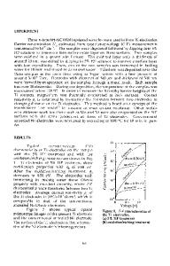
Based on a thermodynamic assessment of the W–In–Ga–As quaternary system, the metal W was selected as a thermodynamically stable ohmic contact material to n-In0.53 Ga0.47 As. As-deposited contacts (on n , 1.4 3 1018 cm23 In0.53 Ga0.47 As) had average specific contact resistances of 7 3 1027 V ? cm2 as measured using the transmission line model. The contact resistances remained unchanged after rapid thermal annealing at 400 ±C for 1 min or at 600 ±C for 1 min, and exhibited no degradation in electrical properties even after long-term annealing at 500 ±C for 100 h. Transmission electron microscopic examination of the contacts showed no interfacial reaction. The present investigation demonstrates the power of thermodynamics in identifying stable ohmic contacts to multicomponent semiconductors.
I. INTRODUCTION
Because of its direct energy band gap, high electron mobility, and high saturated electron drift velocity, the alloy semiconductor In0.53 Ga0.47 As has important applications in high-speed electronic and optoelectronic devices. The achievement of reliable low-resistance ohmic contacts to n-In0.53 Ga0.47 As is essential to the operation of high-performance In0.53 Ga0.47 As devices. Because of the rather small Schottky barrier height of In0.53 Ga0.47 As (,0.25 eV at room temperature1 ), electron transport is very favorable across metal contacts to highly doped n-In0.53 Ga0.47 As. In practice, virtually any metal may serve as an ohmic contact to n-In0.53 Ga0.47 As, if one considers electrical properties alone. However, the thermal stability of a contact material during device processing is also an important factor in the design of contacts to semiconductors. At present, alloyed AuGeNi contacts, which are extensively used as contacts to n-GaAs, are most commonly employed to obtain ohmic contacts on n-In0.53 Ga0.47 As as well. However, this alloyed contact has the disadvantages of poor surface morphology, penetration into the active layer of the device, and a lack of thermal stability, etc.2–4 The same problems occur when AuGeNi is used as a contact for GaAs devices.5,6 J. Mater. Res., Vol. 13, No. 4, Apr 1998
http://journals.cambridge.org
Downloaded: 11 Apr 2015
In recent years, the application of thermodynamic and metallurgical principles has led to significant advances in GaAs contact technology, particularly in the development of solid-state (nonalloyed) contacts. The knowledge of phase equilibria between the met
Data Loading...