Transient Capacitance Studies of a Low-Lying Electron Trap in n-type Silicon
- PDF / 322,029 Bytes
- 6 Pages / 420.48 x 639 pts Page_size
- 8 Downloads / 301 Views
241
TRANSIENT CAPACITANCE STUDIES OF A LOW-LYING ELECTRON TRAP IN n-TYPE SILICON G. E. Jellison, Jr., J. W. Cleland, and R. T. Young Solid State Division, Oak Ridge National Laboratory,* Oak Ridge,
Tennessee 37830
ABSTRACT A new electron trap has been observed in electronirradiated n-type silicon at Ec - ET = 0.105 eV using transient capacitance techniques. It is found that the maximum transient capacitance response is observed only when the majority carrier pulse width is much smaller than some characteristic time constant, and when the time between pulses is much larger than another characteristic time constant. It is shown that this defect is related to an electron trap at Ec-ET = 0.172 eV (probably the oxygenvacancy or A-center); it is believed that this trap is induced by the electric field found in the depletion region of a p-n junction.
INTRODUCTION Electron irradiation-induced defects in n-type silicon have been studied for many years. The work of Watkins, Corbett, and others has resulted in the identification of the oxygen-vacancy defect (A-center) [1,2], the divacancy defect [3], and the phosphorus-vacancy defect (E-center) [4]. The first transient capacitance study of electron-irradiated n-type silicon was performed by Walker and Sah [5]. They found 6 traps in n-type Si, including the A-center at 0.174 eV, the E-center at 0.471 eV, and an unidentified trap at 0.112 eV. Recently, the technique of deep level transient spectroscopy (DLTS) 16] has allowed workers to spectroscopically determine the energy level, capture cross section, and concentration of defects in semiconductors. Kimerling has applied the DLTS technique, in conjunction with annealing studies, to phosphorus-doped silicon, associating specific DLTS peaks to particular traps; in particular, he associated the A-center to a peak at Ec-ET = 0.18 eV [7], and the E-center to a peak at Ec-ET = 0.44 eV [7]. Evwaraye and Sun [8] have shown that two traps at Ec-ET = 0.23 eV and 0.39 eV could be associated with two different charge states of the divacancy. This paper shows that there is another trap in phosphorus-doped silicon at Ec-ET = 0.105 eV which is probably related to the A-center. It will be shown that this new trap disappears under certain pulsing schemes, and is replaced by a trap at Ec-ET = 0.172 eV. Evidence will also be presented showing that this trap is probably activated by the electric field found naturally in the depletion region of the sample diode.
BACKGROUND AND EXPERIMENTAL CONSIDERATIONS Transient capacitance techniques have been used by many workers for the characterization of defects found in the depletion region of junction devices *Operated by Union Carbide Corporation for the U.S. Department of Energy under contract W-7405-eng-26.
242
ORNL-DWG 80-43612
ORNL-DWG80- 11437R TIME
TEMPERATURE (K) 100 90 80 70
120
I
II
I
60
If
/
0•
A•E(eV) 101
E-I1 E-2
Z
0.105 0.172
I
/
100
ia-i k-
LU
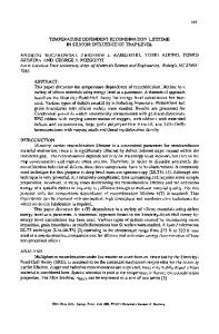
Fig. 1. A schematic of the observed transient capacitance from a majority carrier pulse measured at 77 K of a p+-n diode
Data Loading...