Ultraviolet Photoconductivity of Pure and Al doped ZnO Thin Films by Inkjet Printing
- PDF / 550,046 Bytes
- 6 Pages / 595.22 x 842 pts (A4) Page_size
- 62 Downloads / 317 Views
1161-I03-22
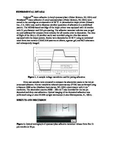
Ultraviolet Photoconductivity of Pure and Al doped ZnO Thin Films by Inkjet Printing Yan Wu, Takahiko Tamaki, Wolfgang Voit, Lyubov Belova, K. V. Rao Department of Materials Science-Tmfy-MSE, Royal Institute of Technology S-100 44 Stockholm, Sweden ABSTRACT Pure ZnO, and Al doped ZnO, 120 -300 nm thin films on glass substrates, were synthesized by inkjet printing technique using zinc and aluminum acetate solution as precursors and a two stage heat treatment process to obtain polycrystalline hexagonal wurtzite structure with the mean grain size of 25 and 30 nm respectively. All films exhibit a transmittance above 85-90% in the visible wavelength range below 700 nm. In the Al doped films the UV absorption spectra show a strong absorption onset below 380nm followed by shoulders centered around 325 nm depending on the film thickness. The electrical conductivity of Al doped ZnO thin films is larger by two orders of magnitude than that for pure ZnO films while the photoconductivity increases by about three orders of magnitude under UV irradiation. The photoresponse of the films with UV irradiation in terms of the rise and decay times in the frequency range from 5 to 500 Hz is also presented and discussed. INTRODUCTION Ink jet printing techniques provide a simple low-cost method to use a solution-process at ambient temperature conditions for developing thin film semiconductors and devices [1-3]. This technique is being extensively used today for various applications in the currently active areas of research such as integrated circuits, transparent electronics, and development of ceramic components, biotechnology, organic light-emitting diodes, and polymers, in addition to conventional graphics applications. Low-cost, nontoxic, environmentally friendly, highly sensitive ultraviolet (UV) sensors are of great interest for the detection of UV light in various special environments. In particular, as a wide band gap (3.3 eV at 300 K) semiconductor with large exciton binding energy (60 meV), ZnO has been intensively studied for such device development [4-6]. The electrical conductivity of pure ZnO thin films is due to either oxygen deficiencies or presence of interstitial Zn in the ZnO lattice. Any additional carrier concentration from a trivalent dopant, (eg. In3+, Al3+, Ga3+ replacing Zn2+) increases the electrical conductivity of the ZnO thin films. However, it is well recognized that the measured electrical conductivity highly depends upon the film deposition technique, crystalline quality of the annealed films, heat treatment schedule, and annealing ambience. Thus, the fabrication of a highly sensitive, inexpensive and large-scale UV sensor using ZnO-based films continues to be a challenge. Although there exist some studies on photoconductivity in pure ZnO, reports on UV photoconductivity in Al doped ZnO films [7-9] are rare, and insufficient to exploit satisfactorily the UV response characteristics. In this paper we present what is perhaps the first early study of UV photoconductivity of pure ZnO and Al doped Z
Data Loading...