Vapor-assisted solution process for perovskite materials and solar cells
- PDF / 520,873 Bytes
- 7 Pages / 585 x 783 pts Page_size
- 21 Downloads / 319 Views
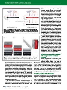
ssisted solution process Perovskite materials typically have the formula ABX3, where A is the organic molecule (CH3NH3+, NH2CHNH2+), B is a divalent metal (Pb or Sn), and X is a halide (Cl, Br, or I). Since the first demonstration of the planar heterojunction architecture, intensive efforts have been devoted to corresponding film formation techniques.30,31 Vacuum and solution processes have become two major methods to fabricate perovskite films starting from inorganic and organic counterparts (e.g., PbX2 and CH3NH3I, respectively). Dual source vapor deposition, where PbCl2 and CH3NH3I, for example, serve as the vapor source, leads to respectable film quality, with compact uniform features in both lateral and vertical directions.14 However, this process requires high-energy consuming vacuum conditions, and the flaky nature of the CH3NH3I powder further makes this deposition method of perovskite films less controllable. Solution processes serve as an alternative method to construct hybrid perovskite films and are based on the simple concept that the material can rapidly form from the solution phase reaction of metal halides (e.g., PbI2) and organic halide salts
668
MRS BULLETIN • VOLUME 40 • AUGUST 2015 • www.mrs.org/bulletin
(e.g., CH3NH3I). However, the film quality obtained from the described simple solution process is typically not satisfactory, resulting in undesired pinholes across the whole film.30,31 This inferior film quality is associated with two key synthetic challenges. The first is a lack of suitable solvents that can simultaneously dissolve both components. The second is the rapid reaction of these two precursors, which prevents the formation of homogenous precursor solutions, even when suitable solvents can be found. To solve this problem, a two-step approach has been demonstrated to fabricate efficient photovoltaic (PV) devices by dipping previously deposited inorganic precursor films into solutions containing the organic species.15,20 This method has been largely successful in films with nanostructured TiO2 scaffolds but has seldom been reported to be applicable for fabricating planar heterojunctions. Growing a CH3NH3PbX3 film with a thickness of several hundred nanometers requires a long reaction time due to the limited surface area of the planar film. The two-step process also leads to strikingly enhanced surface roughness of the films, which frequently peel off from the substrate. To circumvent the aforementioned challenges and construct planar devices with competitive performances, we developed a facile solution approach, VASP,13 for perovskite material formation with enhanced controllability of film quality. VASP takes advantage of the characteristics of the hybrid nature of perovskite materials, particularly the low sublimation temperature of organic halides and the fast reaction rate between the inorganic and organic species. In this method, we make use of the volatile nature of the organic components of the hybrid perovskite films to induce a reaction with the inorganic components while in the vapor phase. Th
Data Loading...