Reduction of dark current in AlGaN/GaN Schottky barrier photodetectors with a low-temperature-grown GaN cap layer
- PDF / 149,426 Bytes
- 6 Pages / 595 x 842 pts (A4) Page_size
- 101 Downloads / 330 Views
Y10.11.1
Reduction of dark current in AlGaN/GaN Schottky barrier photodetectors with a low-temperature-grown GaN cap layer G. C. Chi a), J. K. Sheu1,b), M. L. Lee2), C. J. Kao, Y. K. Su2), S. J. Chang2),and W. C. Lai2) Department of Physics, National Central University Chung-Li 320,Taiwan 1) Institute of Optical Science, National Central University Chung-Li 320,Taiwan 2) Institute of Microelectronics and Department of Electrical Engineering National Cheng Kung University, Tainan 70101,Taiwan a)[email protected] b)[email protected]
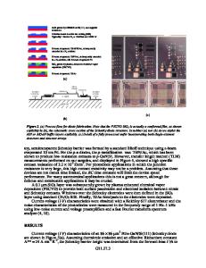
ABSTRACT AlGaN/GaN-based ultraviolet (UV) Schottky barrier photodetectors (PDs) with and without the LT GaN cap layer were both fabricated. It was found that we could achieve a lower leakage current from sample A. With incident light wavelength of 320 nm and a –1 V reverse bias, the measured responsivity was around 0.03 A/W and 0.015 A/W for samples with and without the LT GaN cap layer, respectively. The response speed of the sample A was also found to be faster. INTRODUCTION AlxGa1-xN is one of the most promising materials for the fabrication of high-sensitive visible-blind ultraviolet (UV) photodetectors (PDs), since it has a large direct bandgap energy (3.41~6.2eV at room temperature). The superior radiation hardness and high temperature resistance of AlGaN also make it a suitable material for solar-blind PDs working in extreme conditions. In the past few years, various nitride-based UV PDs have been demonstrated, such as p-i-n PDs, Schottky barrier PDs and metal-semiconductor-metal (MSM) PDs. Compared with bipolar PDs, the fabrication process of Schottky barrier PDs is much simpler. The response speed of Schottky barrier PDs is also faster. However, leakage current in Schottky barrier PDs is also higher due to the large thermionic emission current. To reduce the leakage current in Schottky barrier PDs, it is necessary to achieve a high Schottky barrier height at the metal/semiconductor interface. To our knowledge, various metals [1] and transparent conducting oxides [1] have been deposited onto GaN and/or AlGaN to achieve high performance Schottky barrier UV PDs. Leakage current of Schottky barrier PDs also depends strongly on the properties of the topmost semiconductor layer. Previously, it has been shown that one can significantly reduce gate leakage
Y10.11.2
current in GaAs field effect transistors (FETs) by utilizing a low temperature (LT) GaAs layer [1]. Similar concept has been applied to GaN-based PDs [1]. In this study, we deposited an LT GaN layer on top of undoped AlGaN/GaN. Nitride-based Schottky barrier PDs with the LT GaN cap layer were also fabricated. The optical and electrical properties of the fabricated devices will be reported. EXPERIMENTS Samples used in this study were all grown on c-face (0001) sapphire substrates by organometallic vapor phase epitaxy (OMVPE). We first prepared LT GaN layers and high temperature (HT) GaN layers, respectively. The 0.5µm-thick LT GaN layers were grown directly on sapphire substrates at 560oC. Some of the LT GaN layers w
Data Loading...