Graphene/InP Schottky junction near-infrared photodetectors
- PDF / 1,328,371 Bytes
- 6 Pages / 595.276 x 790.866 pts Page_size
- 52 Downloads / 407 Views
Graphene/InP Schottky junction near‑infrared photodetectors Tao Zhang1 · Jun Chen1 Received: 21 June 2020 / Accepted: 20 September 2020 © Springer-Verlag GmbH Germany, part of Springer Nature 2020
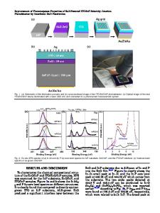
Abstract Graphene and P-type indium phosphide (P-InP) could be combined by van der Waals forces to form a Schottky junction, which can be applied in photodetection. This study reported a graphene/P-InP Schottky junction near-infrared photodetector with a 3-nm-thick Al2 O3 passivation layer and investigated the photoelectric characteristics of such device. As a result, the near-infrared photodetector had a Schottky barrier of 0.89 eV. Besides, this device had a significant response to the wavelength of 808 nm near-infrared light with responsivity and detectivity up to 5.2 mA/W and 1.3 × 1010 cm Hz1∕2 W−1 , respectively, under a reverse bias voltage of 0.4 V. It is expected that the Graphene/P-InP Schottky junction near-infrared photodetector with an Al2 O3 passivation layer may play a vital role in the field of optoelectronic devices in future. Keywords Graphene · InP · Near-infrared detectors · Responsivity
1 Introduction Dangling bond-free or passivated surface has the potential to interact with another surface through van der Waals (vdW) force [1]. Two-dimensional (2D) materials and non-2D materials can be used to form vdW heterojunctions through non-covalent bonds. Graphene, a 2D material, studies have shown that its transmittance constant for visible and infrared light can reach 97.3%, with ultra-high electrical conductivity and carrier mobility, very high Young’s modulus [2–6]. Moreover, in Graphene/semiconductor Schottky junction, a Schottky barrier formed by strong vdW force allows efficient photodetection [7] and the ultra-high transmittance allows more light to be absorbed by the semiconductor. These properties bring great advantages to graphene in the field of optoelectronic applications. In recent years, research on vdW heterostructure devices containing graphene/semiconductor heterostructures, such as graphene/Si [8], graphene/β-Ca2 O3 [9], Graphene/Ge [10], Graphene/gallium arsenide (GaAs) Schottky junction, etc., have become increasingly popular. Luo et al. made a comparison on the responsivity of three different structured near-infrared detectors: device with monolayer graphene (MLG)/GaAs nano-cone structure, * Jun Chen [email protected] 1
School of Electronic and Information Engineering, Soochow University, Suzhou 215006, Jiangsu, China
device with bilayer graphene (BLG)/GaAs structure, and BLG/AlOx /GaAs structured device. They reported the responsivity as 1.73 mA/W, 1.2 mA/W and 5 mA/W, respectively [11, 12]. Wu et al. proposed a near-infrared detector with MLG/GaAs nanowire structure and obtained a response rate of 1.54 mA/W [13]. In Schottky junction photodetector, the separation of photogenerated electron–hole pairs is more likely to occur at higher Schottky barriers. Besides, a high Schottky barrier reduces the recombination of photogenerated carriers [7]. In the application of Graphene/ G
Data Loading...