Defect Reduction in Si-based Metal-Semiconductor-Metal Photodetectors with Cryogenic Processed Schottky Contacts
- PDF / 394,228 Bytes
- 6 Pages / 612 x 792 pts (letter) Page_size
- 5 Downloads / 338 Views
E9.39.1
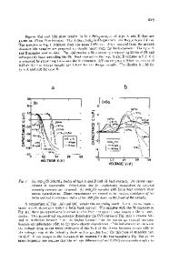
Defect Reduction in Si-based Metal-Semiconductor-Metal Photodetectors with Cryogenic Processed Schottky Contacts M. Li, and W. A. Anderson Department of Electrical Engineering, University at Buffalo, The State University of New York, Buffalo, NY 14260 ABSTRACT Metal-Semiconductor-Metal photodetectors (MSM-PD's) and simple Schottky diodes were fabricated using a low temperature (LT) technique to greatly reduce the device dark current. LT processing for metal deposition increased Schottky barrier height by improving the interface between metal and semiconductor to reduce the leakage current of the device. The structure consists of a 20 Å oxide over the active area to passivate surface states, a thicker oxide under contact pads to reduce dark current and the interdigitated Schottky contacts. A comparison was made for Schottky metal deposited with the substrate at 25 °C or -50 °C (LT). The devices fabricated using the LT process had better I-V characteristics compared to detectors fabricated using the standard room temperature (RT) metal deposition technique. The dark current for the LT film was found to be one to three orders lower in magnitude compared to the film deposited at RT. In one case, for example, the dark current was significantly reduced from 1.69 nA to 4.58 pA at 1.0 V. The active area for the device was determined to be 36 x 50 µm2 with 4 µm electrode width and 4 µm electrode spacing. Additionally, LT-MSM-PD's exhibited an excellent linear relationship between the photo-current and the incident light power. The Schottky barrier height for LT processing was found to be 0.79 eV; however, this value was 0.1 eV more than that of the same contact obtained by RT processing. INTRODUCTION Over the past few years, there has been extensive research on MSM photodetectors on III-V compound semiconductors due to their wide spectral coverage and direct energy band gaps, which allow the ensuing devices to achieve high speeds and good quantum efficiency [1,2]. However, it is difficult and expensive to incorporate them in conventional Si ICs [3]. Silicon, which has an indirect bandgap, is still widely used as the material of choice for the fabrication of photo-devices in Si-based integrated optoelectronic circuits (OEICs), due to its lower cost and the availability of well-established processing technology [4]. Conversely, most Si-based MSMPD's have a higher dark current due to the large thermionic emission current with lateral current flow between two contiguous finger electrodes. The leakage dark current in MSM-PD's can be reduced by Schottky barrier enhancement and fabrication technology. Previous studies show that LT metallization processing provides an alternate way to enhance the Schottky barrier height and reduced carrier trapping at the interfaces between metal and semiconductor [5-7]. In this paper, we present a fabrication procedure for low temperature (LT) processed Sibased MSM-PD's. Both dark and photo current characteristics are compared for both LT and room temperature (RT) MSM-PD's. We also report
Data Loading...