Self-assembled quantum dots and nanoholes by molecular beam epitaxial growth and atomically precise in situ etching
- PDF / 1,561,817 Bytes
- 6 Pages / 612 x 792 pts (letter) Page_size
- 85 Downloads / 285 Views
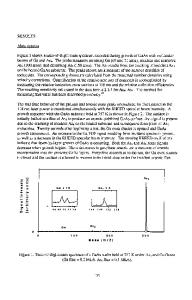
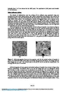
Self-assembled quantum dots and nanoholes by molecular beam epitaxial growth and atomically precise in situ etching S. Kiravittaya, R. Songmuang, and O. G. Schmidt Max-Planck-Institut für Festkörperforschung, Heisenbergstraβe 1, D-70569 Stuttgart, Germany. ABSTRACT Ensembles of homogeneous self-assembled quantum dots (QDs) and nanoholes are fabricated using molecular beam epitaxy in combination with atomically precise in situ etching. Self-assembled InAs QDs with height fluctuations of ±5% were grown using a very low indium growth rate on GaAs (001) substrate. If these dots are capped with GaAs at low temperature, strong room temperature emission at 1.3 µm with a linewidth of 21 meV from the islands is observed. Subsequently, we fabricate homogeneous arrays of nanoholes by in situ etching the GaAs surface of the capped InAs QDs with AsBr3. The depths of the nanoholes can be tuned over a range of 1-6 nm depending on the nominal etching depth and the initial capping layer thickness. We appoint the formation of nanoholes to a pronounced selectivity of the AsBr3 to local strain fields. The holes can be filled with InAs again such that an atomically flat surface is recovered. QDs in the second layer preferentially form at those sites, where the holes were initially created. Growth conditions for the second InAs layer can be chosen in such a way that lateral QD molecules form on a flat surface.
INTRODUCTION The growth of self-assembled quantum dots (QDs) in the Stranski-Krastanow mode has been of broad interest in recent years due to potential applications in the field of opto-electronics. [1-3]. Several growth techniques such as the usage of a very low InAs growth rate are available to fabricate homogeneous ensembles of QDs, which emit at 1.3 µm [4-6]. Further manipulation of buried QDs is feasible by applying in situ etching techniques [7,8]. In this article, we report about the fabrication of homogeneous InAs QD arrays with narrow luminescence linewidth and a systematic investigation of an in situ etching procedure of capped QD. The AsBr3 in situ etching gas produces nanoholes in the GaAs capping layer. These hole structures can be filled with InAs again to produce lateral QD molecules in the second layer.
EXPERIMENT Growth is carried out in a modified RIBER solid source molecular beam epitaxy chamber integrating an AsBr3 in situ etching gas system. The detailed setup of the etching gas system has been described elsewhere [8]. All sample structures were grown on semi-insulating GaAs (001) substrate under constant As4 pressure of 8×10⁻⁶ mbar. After desorbing the oxide at a substrate temperature Ts = 640°C, a 400-nm GaAs buffer, 20-nm Al0.4Ga0.6As, and a 20-nm GaAs layer were deposited at Ts = 610°C. The growth rates of GaAs and Al0.4Ga0.6As were 0.6 and 1.0 ML/s, respectively. An 1.8 ML InAs self-assembled QD layer was deposited at Ts = 500°C using K10.11.1 Downloaded from https://www.cambridge.org/core. Access paid by the UCSB Libraries, on 19 Jul 2018 at 10:34:16, subject to the Cambridge Core terms of use, availabl
Data Loading...