Synthesis of Silicon Nanowires and their Heterostructures by Thermal Chemical Vapor Deposition
- PDF / 739,545 Bytes
- 4 Pages / 595 x 842 pts (A4) Page_size
- 89 Downloads / 360 Views
Z7.25.1
Synthesis of Silicon Nanowires and their Heterostructures by Thermal Chemical Vapor Deposition Woo-Sung Jang, Seung Yong Bae, and Jeunghee Park* Department of Chemistry, Korea University, Jochiwon 339-700 Korea;
ABSTRACT The Si nanowires were synthesized using a novel catalytic thermal reaction under Ar flow. The average diameter is in the range of 50 ~ 100 nm. They consist of defect-free single-crystalline cubic structure with the [111] growth direction. The thickness of amorphous oxide outer layers was controllable by growth conditions or surface treatment. In order to protect the oxidation, the Si nanowires were coated with boron nitride layer by the reaction of boron oxide mixture with NH3. INTODUCTION One-dimensional nano-materials, including silicon nano-wires (SiNWs), are arousing much interest due to their importance in physics and chemistry [1.4]. Because of the quantum confinement effect, SiNWs showed many unusual electronic and optic properties [5.7] and may play an important role on nano-devices in future. Up to now, several techniques have been developed to fabricate random SiNWs, such as laser ablation [8], thermal evaporation with catalyst [9.11], electronic-chemical method [12]. In recent, arrayorderly SiNWs fabricated by nano-channel-Al2O3 (NCA) and chemical-vapor-deposition (CVD) process via vapor-liquidsolid (VLS) mechanism were also reported [13.16]. However, there are still many challenges for the application of SiNWs, for example, precise controllable growth of SiNWs on silicon wafers.
EXPERIMENTAL DETAILS The n-type Si (100) substrates with an area of 10-20 cm2 were coated with 0.001M AuCl2·4H2O (99%, Aldrich) etanol solution. The thickness of AuCl2 film was about 300 nm. The substrate was loaded cooling zone in a quartz tube reactor. Si powder (99.99%, Aldrich) was placed near to the substrates. Argon was flowed into the tube reactor while raising the temperature at a rate of 300-500 sccm. The temperature of the substrates was set at 1200 oC and the growth time was 30 min – 1h. The size and structure of the products were examined by scanning electron microscopy (SEM, Hitachi S-4300), transmission electron microscopy (TEM, Jeol JEM-2010), selected-area electron diffraction (SAED), and X-ray powder diffraction (XRD, Philips X’PERT MPD).
Z7.25.2
RESULTS AND DISCUSSION
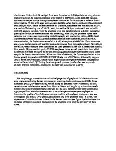
Figure 1. (a) SEM micrograph for the Si-NWs grown on silicon substrate using a reaction of Si powder/substrate and Ar. (b) SEM image for a number of Si-NWs, showing the average diameter of 75 nm. (c) TEM images and its corresponding electron diffraction of a Si-NW whose wire axis is perpendicular to [-111]. (d) A magnified view of (c) showing defect free (111) planes. Figure 1(a) is a SEM image for the high-density NWs grown homogeneously over a large area of substrate. The NWs have very clean surface without any particles. A side view reveals that the NWs are grown with a length of about 2-4 µm. Figure 1(b) is SEM image showing a typical morphology of Si-NWs. They have nearly uniform diameters with a mean value of 7
Data Loading...