Strain-Transfer Structure Beneath the Transistor Channel for Increasing the Strain Effects of Lattice-Mismatched Source
- PDF / 172,630 Bytes
- 6 Pages / 612 x 792 pts (letter) Page_size
- 98 Downloads / 366 Views
0995-G01-03
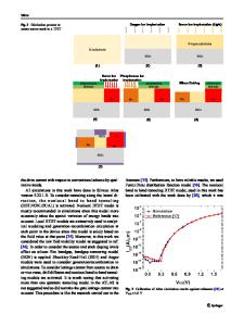
Strain-Transfer Structure Beneath the Transistor Channel for Increasing the Strain Effects of Lattice-Mismatched Source and Drain Stressors Yee-Chia Yeo, Kah-Wee Ang, Jianqiang Lin, and Chee-Shing Lam Dept. of Electrical and Computer Engineering, National University of Singapore, 4 Engineering Drive 3, Singapore, 117576, Singapore ABSTRACT We incorporate an additional semiconductor heterostructure beneath the transistor channel region to increase the strain-transfer efficiency of lattice-mismatched source/drain (S/D) stressors, resulting in higher strain levels in the channel region. The additional structure is lattice-mismatched with respect to the overlying Si-channel and/or with respect to the S/D stressors. For an n-FET with Si:C S/D, a SiGe region integrated beneath the Si-channel enhances the magnitude of the tensile strain in the channel region. For a p-FET with SiGe S/D, a Si:C region beneath the Si-channel enhances the strain effect in the channel region. This additional structure beneath the transistor channel is called a strain-transfer structure (STS). Extensive numerical simulations were performed using the finite element method to explain how the new strain-transfer structure works. Profiles of the various strain components in the transistor channel were obtained. Dependence of the strain effect on geometrical features of the new transistor structure will also be reported. INTRODUCTION Incorporating strain in the channel of metal-oxide-semiconductor field-effect transistors (MOSFETs) enables the achievement of higher carrier mobilities and drive current performance [1-2]. When materials that are lattice-mismatched with respect to the channel are incorporated in the source/drain (S/D) regions, lattice interactions between the S/D material and the channel material can be exploited for the realization of strained-Si transistors. For Si channel transistors, silicon-germanium (SiGe or Si1-uGeu) S/D generates compressive stress for hole mobility enhancement [2], while silicon-carbon (Si:C or Si1-vCv) S/D results in tensile stress for electron mobility enhancement [3-4]. Very recently, a new device heterostructure with an embedded SiGe region beneath a Si channel, also known as reverse-SiGe region, was demonstrated to induce tensile strain in the longitudinal direction for electron mobility enhancement [5]. In this structure [Figure 1(a)], lattice interactions at the SiGe/Si vertical heterojunction between the embedded SiGe structure and the Si S/D region causes a vertical compression of the SiGe lattice. This results in a reduced horizontal or lateral compression in the SiGe lattice as compared to its as-grown fully strained state, leading to a transfer of a lateral tensile strain to the overlying Si channel region. This concept can be applied in a transistor with lattice-mismatched S/D regions. In this paper, we incorporate a heterostructure or a strain-transfer structure (STS) beneath the transistor channel and in between the lattice-mismatched source/drain stressors to increase the strain in
Data Loading...


