Thermal Evolution of Extrinsic Defects in Ion Implanted Silicon: Current Understanding and Modelling
- PDF / 319,221 Bytes
- 12 Pages / 612 x 792 pts (letter) Page_size
- 96 Downloads / 334 Views
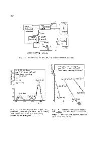
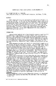
Thermal Evolution of Extrinsic Defects in Ion Implanted Silicon: Current Understanding and Modelling Fuccio Cristiano, Benjamin Colombeau*, Bernadette de Mauduit, Caroline Bonafos, Gerard Benassayag and Alain Claverie Ion Implantation Group CEMES-LAAS/CNRS Toulouse - CEMES/CNRS, 29, rue J.Marvig, 31055 Toulouse, France - LAAS/CNRS, 7 Ave. Colonel Roche, 31077 Toulouse, France * Current address: School of Electronics, Computing and Mathematics, Univ. of Surrey, UK ABSTRACT We present an extensive study of the thermal evolution of the extended defects found in ion implanted Si as a function of annealing conditions. We will first review their structure and energetics and show that the defect kinetics can be described by an Ostwald ripening process whereby the defects exchange Si atoms and evolve in size and type to minimise their formation energy. Finally, we will present a physically based model to predict the evolution of extrinsic defects during annealing through the calculation of defect densities, size distributions, number of clustered interstitials and free-interstitial supersaturation. We will show some successful applications of our model to a variety of experimental conditions and give an example of its predictive capabilities at ultra low implantation energies. INTRODUCTION The continuous evolution of ICs towards smaller sizes requires the reduction of both the lateral and the vertical device dimensions. In particular, the junction depths of source and drain extension must decrease well below 50 nm [1]. While new strategies of shallow junction formation are being investigated (plasma doping; laser anneals, heavy ions…) [2,3], it is expected that the conventional ion “implantation + RTA” procedure will still be used (and pushed to its limits) for the next future. This will be achieved by the use of ULE implants (< 1 keV), preamorphisation with Ge+ or Si+ ions and “spike” anneals with ultra fast ramp up times[4]. In these conditions, the major obstacle to the fabrication of such shallow junctions remains the well known phenomenon of Transient Enhanced Diffusion (TED) of dopants, in conjunction with the formation of extended defects of various types (including dopant-interstitial clusters) following an ion implantation step [5]. At the same time, physical models are needed to improve the reliability of predictive process simulation tools. In this paper, we will focus on the various aspects related to the formation of extended defects in ion implanted silicon. The aim is, on one hand, to review our knowledge of the structure and thermal behavior of the different types of extended defects which can be formed by ion implantion and thermal annealing in silicon and, on the other hand, to understand the interactions between these defects and the dopant atoms that are at the origin of the TED phenomenon. In a first part, we will present an extensive study of the thermal evolution of the extended defects and we will discuss their thermal behaviour on the basis of TEM analysis. We will show that the defect kinetics can
Data Loading...