Sub-micron structured Metal Oxide gas sensors by means of lithographic techniques
- PDF / 392,450 Bytes
- 6 Pages / 612 x 792 pts (letter) Page_size
- 12 Downloads / 258 Views
A2.8.1
Sub-micron structured Metal Oxide gas sensors by means of lithographic techniques Patrizio Candeloro, Camilla Baratto, Elisabetta Comini, Guido Faglia, Enzo M. Di Fabrizio1, Giorgio Sberveglieri Sensor Lab – INFM, Chemistry and Physics department, University of Brescia, via Valotti 9, 25133 Brescia, Italy 1 LILIT Beamline, TASC – INFM, S.S.14 km163.5, 34012 Basovizza (TS), Italy ABSTRACT In this work we employed lithographic techniques, combined with sputtering depositions, to fabricate semiconductor metal-oxide (MOX) gas sensors with controlled grain dimensions. The basic idea is to replace the continuous sensing film of standard MOX sensors with a pattern of wires in the sub-micron scale, thus controlling the lateral size of the grains. Regarding the fabrication process, we followed two different approaches: a plain lift-off technique and a substrate patterning process. We present a comparison between the results of both the approaches. Furthermore, we tested the electrical responses to several gases and compared them with those of continuous film sensors. The experimental data highlight an improvement for the patterned sensors.
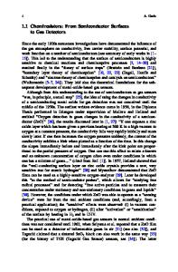
INTRODUCTION Nowadays continuous layers of polycrystalline semiconductor metal oxide (MOX), such as SnO2, WO3 and TiO2, are widely used in gas sensor technology [1]. The sensing mechanism allows to detect modifications in the external atmosphere by means of electrical measurements; in fact, due to the presence of different external gases, the MOX film changes its electrical properties, like the conductivity. This is due to a surface phenomenon: in room-air, oxygen adsorbs at the semiconductor surface and produces an electron depletion layer (for a n-type semiconductor); as a consequence an energy barrier, eVS, for the grain-to-grain current arises. The thickness, L, of the depletion layer is obviously related to the oxygen partial pressure, but also to the temperature and the Debye screening length. In presence of a reducing gas, an amount of oxygen desorbs, thus leading to a lowering of both the depletion layer thickness and the barrier height. The result is a modification of the semiconductor electrical properties, like the conductivity, and variations of the atmosphere surrounding the sensor are detected by means of conductance measurements. The sensitivity of this mechanism is strongly grain-size dependent: the smaller the grain the larger the sensitivity [2]. Each grain of a polycrystalline film presents a depleted layer; when the grain size, D, has dimensions comparable with 2L, a complete depletion of carriers occurs. Consequently the transport properties of the material are dramatically changed and an enhancement of the sensitivity is observed [3]. For this reason the microscopic morphology of the material plays a key-role and several studies of nanostructured oxides have been presented [4]. In this work lithographic techniques combined with sputtering depositions are employed to fabricate metal-oxide sensors with controlled grain dimensions. While the sensing layer of
A
Data Loading...