Surface and Interface Analysis of Thin-Film/Si(Substrate) Contacts by Sxes
- PDF / 376,870 Bytes
- 6 Pages / 414.72 x 648 pts Page_size
- 34 Downloads / 302 Views
377 Mat. Res. Soc. Symp. Proc. Vol. 448 ©1997 Materials Research Society
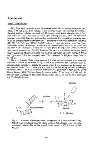
A thin-film/Si(substrate) contact specimen was prepared by either a solid phase reaction(SPR) or a chemical vapor deposition(CVD). A silicon compound film was prepared by the former method, where a thin film of a component material was first deposited on a Si substrate to be followed by a heat treatment below melting points of either constituent materials or the compound to be grown. XPS study was done with a commercially available apparatus. RESULTS AND DISCUSSION Si-K 03emission band spectrum is shown in Fig.1(a) for CrSi2, where the signal is normalized at the highest peak and plotted as a function of photon energy(h v ). The features to be noted in the spectrum for CrSi2[Fig.1(a)] is that it has a peak at h v -1836.6eV with a shoulder at -'1834.2eV. This is a clear difference from the fact that the Si-K 13emission band spectrum of a Si crystal has a peak at -,1836.9eV. Cr3Si, another compound phase in the Cr-Si binary system, showed a Si-K 13 emission band spectrum with a peak at - 1834.2eV, which is different from either that of a Si crystal or the one of CrSi2. This kind of difference in the spectral shape among a Si crystal and Cr-silicides can be used as finger prints to identify what kind of material exists on top or at the interface of a thinfilm/substrate contact system. Cr(thin-film, 50- 100nm)/Si(100) specimens heat treated at different temperatures have been studied. In Ep =5 keY Fig.1 Si-K 13emission band spectra are .r4 shown for CrSi2(a) and the specimens heat treated at 450(b) and 425°C(c), where the incident electron energy is (a) 5keV. The spectra of Fig.l(a)-(c) are quite similar. Therefore, one can claim .6 that CrSi2 like compounds are formed for Cu the specimen heat treated at 450 and 425 (b) : OC. C') Si- L2, 3 emission band spectra are a) 4-. shown in Fig.2 for CrSi2(a) and Cr(thinfilm)/Si(substrate) specimens heat treated at 450(b) and 4250C(c), where detected photons are plotted as a function of the photon energy(h v ). Here, it should be 1820 1830 1840 noted that the Si L2,3 emission band Photon energy (eV) spectrum reflects the VB-DOS with sand/or d-symmetry according to the Fig.1 Si-K 13emission band spectra: CrSi2(a), and dipole selection rule, because the specimens of Cr(film)/Si(100) heat treated at signal of the photon emission cor450°C(b) and 4250C(c).
378
responds to the electron transition from the valence band to the Si(2p) core holes. On the other hand, the Si-K 13emission band spectrum gives information on the partial VB-DOS of Si-p electronic states. The spectrum of Fig.2(a) for CrSi2 has the following characteristics, i.e., it has two broad peaks at h v ---91.4 and 96.7eV, which is a clear difference from the fact that Si-L2,3 spectrum for a Si crystal have a double peak at h v -89 and 92eV and a terrace that extends to the top of the valence band[3]. There are clear differences between the spectrum for CrSi2 and the one for a Si crystal. Si-L2,3 emission band spectrum for Cr3Si has a peak at -90
Data Loading...