Synthesis of Nano/Meso-Structured Silicon Films by Plasma Deposition
- PDF / 1,855,370 Bytes
- 6 Pages / 612 x 792 pts (letter) Page_size
- 91 Downloads / 397 Views
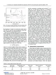
Figure 1. (a) Cube plot for the three factors and (b) thickness of the silicon films as a function of dilution ratio.
Structural, electrical and optical properties were studied. Absorption spectra and optical gap were estimated by transmittance using a Perkin-Elmer Lambda 3B spectrophotometer in the UV-Vis region. Bonding structure was studied by infrared spectroscopy (IR) in the MIR region, using a Bruker spectrometer model Vector-22. The Raman crystallinity factor was determined by Raman spectroscopy, by means of a Horiba Jobin Yvon HR800 instrument. Surface roughness and morphology were analyzed by Atomic Force Microscopy (AFM) using a Nanosurf easy-scan DFM. Dark conductivity was obtained by current-voltage sweep, I(V), with a Keithley 6517A electrometer and the transmission line method. For photoconductivity measurements, the samples were illuminated using an ORIEL sol 2A class ABA solar simulator (AM1.5 spectrum). RESULTS Structural characteristics Figure 2(a) shows the absorbance spectra obtained by IR measurements. The hydrogen content, CH, was calculated by using the wagging mode located at 640 cm-1 [11].The microstructure parameter, R*, was determined from the analysis of the stretching vibration modes, by R*=IHSM/(LLSM + IHSM), where ILSM and IHSM are the integrated absorption of low stretching mode (LSM) located around of 2000 cm-1, and high stretching mode (HSM) located at the range of 2060-2160 cm-1 [2,11]. Medium stretching mode (MSM) located at 2030 cm-1 is attributed to silicon nanocrystalline surfaces in polymorphous silicon. A Gaussian peak at 2016 cm-1 can be seen as a combination of LSM and MSM [10]. In the IR spectra of the synthesized silicon films were observed the three contributions of LSM, MSM and HSM. Figure 2(b) shows the Raman spectra of the films. The Raman crystallinity factor is a ratio of Raman intensities, it is given by: C=(I520+I510)/(I520+I510+I480), where Ii denotes the integrated intensity centered at the i position (480, 510 and 520 cm-1) which corresponds to a-Si:H, nc-Si:H and c-Si respectively [12]. The region of 500-520 cm-1 is correlated to the presence of nanocrystals of size between 2-20 nm [13]. The samples at low-H2 level (HSiP-0XX, i.e. R=0.5 and R=5) showed these features. The contribution of MSM in IR spectra confirmed the formation of nanocrystals.
Figure 2. (a) Absorbance spectra from IR measurements and (b) Raman spectra.
Figure 3 shows the AFM images of the silicon films. Significant variations are observed in the scanned area (3×3 µm2). RMS roughness, particle size and density were determined by Scanning Probe Image Processor (SPIP). Meso-structures in the range of 250-350 nm were determined for the samples at low-H2 level (HSiP-0XX, i.e. R=0.5 and R=5). It is known that roughness of µc-Si:H films increases (~16 nm) [2]. In this sense, as-deposited silicon films with high roughness in the range of 20-36 nm were obtained without any post-deposition treatment.
Figure 3. AFM images of the surface of the silicon films.
Optoelectronic properties We obtained
Data Loading...