TEM Study of strain states in III-V semiconductor epitaxial layers
- PDF / 1,188,105 Bytes
- 6 Pages / 595 x 842 pts (A4) Page_size
- 58 Downloads / 268 Views
TEM Study of strain states in III-V semiconductor epitaxial layers. André ROCHER, Anne PONCHET, Stéphanie BLANC* and Chantal FONTAINE*. Centre d'Elaboration de Matériaux et d'Etudes Structurales, CEMES/CNRS, BP 4347, Toulouse, F-31055, France. *Laboratoire d’Analyse et d’Architecture des Systèmes, LAAS/CNRS, 7 av. Colonel Roche, Toulouse, F-31077, France. ABSTRACT The strain states induced by a lattice mismatch in epitaxial systems have been studied by Transmission Electron Microscopy (TEM) using the moiré fringe technique on plane view samples. For the GaSb/(001)GaAs system, moiré patterns suggest that the GaSb layer is free of stress and homogeneously relaxed by a perfect square array of Lomer dislocations. A 10 nm thick layer of GaInAs (20% In concentration) grown on (001)GaAs does not give any moiré fringes for all low-index Bragg reflections: this result indicates that the effective misfit strain does not correspond to the theoretical one described by the elastic theory. Segregation effects are expected to play an important role in the relaxation of the misfit strain. INTRODUCTION The strain induced by a lattice mismatch in epitaxial systems is known to control the main physical properties of quantum wells. For epitaxial structures, such strains are assumed to be perfectly pseudomorphic when misfit dislocations are absent at the interface. A TEM technique for studying the misfit strain is described in this article. It is based on the moiré phenomenon, which is very sensitive for evaluating the lattice parameter of an epitaxial layer relative to that of the substrate. The crystalline quality of a layer is directly characterized, with the conventional TEM resolution, by the homogeneity of the moiré pattern. Comparison of the experimental and theoretical values of the lattice parameters allows us to evaluate locally the epitaxial strain. Two systems are studied: the GaSb/(001)GaAs, fully relaxed by a perfect misfit dislocation network, which gives rise to well defined moiré patterns, and GaInAs/(001)GaAs, where the strain has to be measured. ANALYSIS OF MISFIT STRAIN All models of epitaxial strain are based on elasticity theory, the crystalline perfection of the epitaxial layer and the hypothesis of a perfect interface with perfect bonding. For cubic crystals, the lattice mismatch is defined as m = (a - b)/a, where a and b are the film and substrate lattice parameters. At the onset of epitaxy, the film takes the same crystalline orientation as the substrate. When the film is assumed to be pseudomorphic, i.e. elastically strained (Fig.1), the planes normal to the interface have exactly the same spacing in both the layer and the substrate. For the (001) interface, the distortion is tetragonal and the strain ε// and ε ⊥ components calculated by the elasticity theory are given by:
P5.5.1
as
dl
al
ds b
d
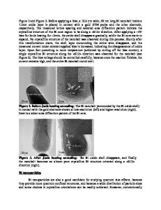
Figure 1: Diagram of the pseudomorphic (solid lines) and relaxed (dotted lines) unit cells (m>0).
ε// = ε100 = ε010 = − m
and
ε ⊥ = ε001 = − ε// ∗ (2C12/C11)
In ΙΙΙ−V compounds, ε ⊥ ≈ 0.9 m. The ε ⊥ and ε//
Data Loading...