TEM study of the structure and chemistry of a diamond/silicon interface
- PDF / 1,218,490 Bytes
- 7 Pages / 576 x 792 pts Page_size
- 21 Downloads / 327 Views
J. Bruley,a) F. Ernst, and M. Riihle Max-Planck-Institut fur Metallforschung, Institut fur Werkstoffwissenschaft, Seestrafie 92, 70174 Stuttgart, Germany
R. Raj Department of Materials Science and Engineering, Cornell University, Ithaca, New York 14853-1501 (Received 9 August 1993; accepted 10 February 1994)
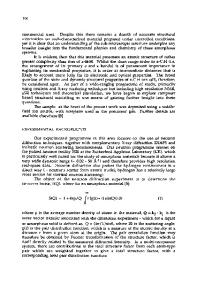
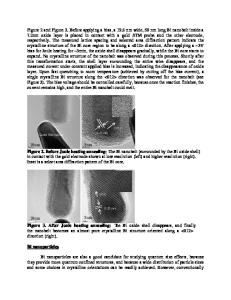
The interface between diamond and silicon, fabricated by growing diamond films on (001) silicon by microwave plasma assisted chemical vapor deposition (MPACVD), was characterized by high-resolution transmission electron microscopy (HRTEM) and electron energy loss spectroscopy (EELS). Two types of interface morphology were identified. Type A interfaces contain an amorphous transition layer composed of silicon, carbon, and oxygen; the diamond overgrowth on this layer consists of nanocrystalline grains with random orientations. Type B interfaces consist of large diamond grains having special orientations with respect to the silicon substrate, without an obvious presence of a glassy phase and with a much lower oxygen content than type A interfaces.
I. BACKGROUND While diamond films are now being routinely synthesized by CVD, 1 it has not yet been possible to grow heteroepitaxial diamond on semiconductors, which would be of interest in electronic applications. In this paper we report a detailed TEM study of the diamond/ silicon interface where, in some regions, large single crystals of diamond with special orientation with respect to the silicon were observed. The specimen also contained regions where the interface was obviously amorphous and the diamond overgrowth was nanocrystalline. In the following discussion, the glassy interfaces are called type A boundaries and the special, pseudo-heteroepitaxial interfaces are described as type B interfaces. In type A interfaces the chemistry of the glass is of the greatest interest, and is explored by EELS in Scanning-TEM, whereas in type B interfaces the structural relationship between the Si and the diamond is of interest and was studied by HRTEM. II. SPECIMEN PREPARATION The diamond films studied in this work were grown by MPACVD. Single crystal (001) silicon substrates were scratched with 1 /xm diamond paste before deposition. During the deposition the substrate was heated a 'Present
address: Department of Materials Science and Engineering, Lehigh University, Whitaker Laboratory #5, Bethlehem, Pennsylvania 18015-3195.
1566 http://journals.cambridge.org
J. Mater. Res., Vol. 9, No. 6, Jun 1994 Downloaded: 12 Dec 2014
by a plasma and was maintained at a fixed temperature as measured by optical pyrometer. The reactant gas was 1% methane in hydrogen; the pressure in the reaction chamber was maintained at 50 Torr. Films were prepared in two ways. In one, the films were deposited in two steps: first it was grown for 1 h at a low temperature (between 500 °C and 700 °C), followed by further growth for 1 h at a high temperature (between 700 °C and 900 °C). In the other method the films were grown at one temperature (900 °C) for 2 h. Cross-section TEM specimens were prepare
Data Loading...