The Effects of Device Dimension, Substrate Temperature, and Gate Metallization on the Reliability of AlGaN/GaN High Elec
- PDF / 1,248,497 Bytes
- 12 Pages / 612 x 792 pts (letter) Page_size
- 95 Downloads / 258 Views
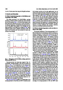
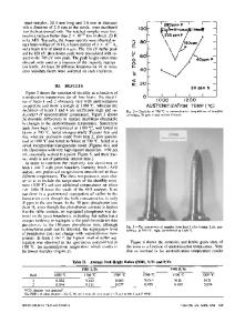
The Effects of Device Dimension, Substrate Temperature, and Gate Metallization on the Reliability of AlGaN/GaN High Electron Mobility Transistors F. Ren1, S. J. Pearton2, Lu Liu1, T.-S. Kang1, E. A. Douglas2, C. Y. Chang2, C.-F. Lo1, D. A. Cullen3, L. Zhou3, and D. J. Smith3 1 Department of Chemical Engineering, University of Florida, Gainesville FL 32611 2 Department of Materials Science and Engineering, University of Florida, Gainesville FL 32611 3 Department of Physics, Arizona State University, Tempe, AZ 85287 ABSTRACT The effects of source field plates on AlGaN/GaN High Electron Mobility Transistor reliability under off-state stress conditions were investigated using step-stress cycling. The source field plate enhanced the drain breakdown voltage from 55V to 155V and the critical voltage for off-state gate stress from 40V to 65V, relative to devices without the field plate. Transmission electron microscopy was used to examine the degradation of the gate contacts. The presence of cracking that appeared on both source and drain side of the gate edges was attributed to the inverse piezoelectric effect. In addition, a thin oxide layer was observed between the Ni gate contact and the AlGaN layer, and both Ni and oxygen had diffused into the AlGaN layer. The critical degradation voltage of AlGaN/GaN High Electron Mobility Transistors during off-state electrical stress was determined as a function of Ni/Au gate dimensions (0.1-0.17μm). Devices with different gate length and gate-drain distances were found to exhibit the onset of degradation at different source-drain biases but similar electric field strengths, showing that the degradation mechanism is primarily field-driven. The temperature dependence of sub-threshold drain current versus gate voltage at a constant drain bias voltage were used to determine the trap densities in AlGaN/GaN high electron mobility transistors (HEMTs) before and after the off-state stress. Two different trap densities were obtained for the measurements conducted at 300-493K and 493-573K, respectively. INTRODUCTION The promising performance of AlGaN/GaN High Electron Mobility Transistors (HEMTs) under high frequency and high output power density conditions has intensified efforts to understand reliability and degradation mechanisms under different operating conditions [1-13]. At high source-drain biases, crystallographic defects and even cracking can occur as a result of the inverse piezoelectric effect [2-7]. Under these conditions, the presence of strong electrostatic fields in the piezoelectric GaN and AlGaN layers leads to additional mechanical stress that is concentrated in the AlGaN barrier layer. At high enough field, the change in AlGaN elastic energy can produce extended and point defects. The degradation under off-state conditions is electric-field driven, with devices of different gate length failing at different drain-source biases but similar electrostatic field thresholds. Field plates have been employed for AlGaN/GaN HEMT and GaAs Metal Semiconductor Field Effect Transistors
Data Loading...