The Improvement of Bonding Metal Layers in a GaAs Vertical Structure Light-Emitting Diode Package
- PDF / 3,668,940 Bytes
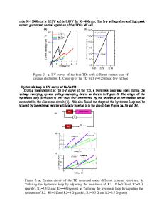
- 6 Pages / 593.972 x 792 pts Page_size
- 1 Downloads / 292 Views
https://doi.org/10.1007/s11664-020-08359-5 Ó 2020 The Minerals, Metals & Materials Society
INTERNATIONAL ELECTRON DEVICES AND MATERIALS SYMPOSIUM 2019
The Improvement of Bonding Metal Layers in a GaAs Vertical Structure Light-Emitting Diode Package YING-CHANG LI,2 LIANN-BE CHANG ,1,2,3,4,6 MING-JER JENG,2,3 TZER-EN NEE,1,5 JANG-HSING HSIEH,4 CHIA-NING CHANG,1 HAO-ZONG LUO,1 and YU-CHI LI1 1.—Graduate Institute of Electro-Optical Engineering, Chang Gung University, Taoyuan City 33302, Taiwan. 2.—Green Technology Research Center, Chang Gung University, Taoyuan City 33302, Taiwan. 3.—Department of Otolaryngology-Head and Neck Surgery, Chang Gung Memorial Hospital, Linkou, Taoyuan 333, Taiwan. 4.—Department of Materials Engineering, Ming-Chi University of Technology, New Taipei City 24301, Taiwan. 5.—Department of Oral and Maxillofacial Surgery, Linkou Chang Gung Memorial Hospital, Kwei-Shan, Tao-Yuan 333, Taiwan. 6.—e-mail: [email protected]
This paper presents an investigation into the reliability of substrate bonding between metal layers and gallium arsenide vertical-injection light-emitting diodes (GaAs VLEDs). In this study, molybdenum (Mo) acts as a buffer layer between the GaAs VLED and the aluminum-based metal core printed circuit board (MCPCB). The thermal expansion coefficient (CTE) value of GaAs is approximately equal to that of the Mo layer under the substrate. This is beneficial for slowing the decay of the adhesive bond due to temperature cycling from 40°C to 125°C for 50 cycles. The experimental results show that the use of the Mo buffer layer greatly improved the electrical and optical performance of the LED packages. The average leakage current was reduced from 33.63 mA to 2.37 mA at the reversed voltage of 3 V and the increase in light output power was 130% at an injection current of 0.7 A. The results also show that a Mo buffer layer can reduce the risk of cracking on bonding wires after the thermal shock test (TST). These results are useful for improving the aging of GaAs VLEDs. Key words: GaAs, light-emitting diode (LED), vertical-injection light-emitting diodes (VLEDs), thermal shock test (TST)
INTRODUCTION Currently, the development of light-emitting diode (LED) technology is becoming more mature, with a focus on high luminosity and small volumes.1 Therefore, trends towards high luminous flux and size miniaturization, such as the research of miniLED and micro-LED technology, are evident within the LED light market.2,3 Both trends increase power density and generate uncontrolled heat in
(Received December 5, 2019; accepted July 24, 2020)
LED devices, which has led to heat management becoming both a critical and essential issue for the performance of next generation LED technology.4–7 Excessive junction temperature of the LED may degrade the life, efficacy, and brightness of a chip. Many techniques are being developed to overcome this challenge. Xiao et al. proposed a design combining a gallium arsenide (GaAs)LED with a photovoltaic cell, in which luminescent photons act as the working fl
Data Loading...