The Influence of Tiw Barrier Layer on Reliability of AlCu and AlSiCu Interconnects
- PDF / 2,522,153 Bytes
- 6 Pages / 414.72 x 648 pts Page_size
- 108 Downloads / 560 Views
ABSTRACT The influence of a TiW barrier layer on the stress-voiding behavior of AlCu and AlSiCu interconnects is investigated. The results are compared to the same alloys deposited on Si0 2. In both cases, AlCu exhibits a notably better voiding behavior compared to AlSiCu. In the case in which the alloys are directly deposited on the TiW barrier without breaking vacuum between TiW and Al(Si)Cu depositions, a significant improvement of the voiding behavior of both alloys is observed. Compared to AICu, AlSiCu shows worse voiding behavior due to the presence of Si precipitates, which introduce significant extra dislocations and defects in the Al grains. These dislocations and defects are diffusion paths which assist stress relaxation and void formation. In the presence of a TiW barrier part of the Si content of the A1SiCu is consumed during the anneal by the A1-TiW interface, which results in a decreased number of dislocations and defects within the Al grains, and an improved voiding behavior compared to AlSiCu on Si0 2. Furthermore, W and Ti diffuse into the grain boundaries of both alloys. The presence of W and Ti in the grain boundaries reduces the amount of Cu depletion from within the grains, which makes both alloys more resistant to stress voiding. The above is supported by Auger and TEM results. The electromigration results of the alloys in question are presented. These show that also with respect to electromigration AlCu is the preferred alloy both on TiW and Si0 2. INTRODUCTION The integrated circuit (IC) industry's continuous drive towards higher device densities on the chip and towards faster circuits increases the importance of IC metallization reliability issues such as stress voiding and elec473 Mat. Res. Soc. Symp. Proc. Vol. 391 01995 Materials Research Society
On SiO 2
On TiW
Alloy
MTF o,
MTF or
AICu AlSiCu
67 60
AlSiCu on SiO 2 AICu
0.86 0.94
223 18
0.62 0.4
Table I Results of electromigration tests. Tested lines were 1.2 um wide. MTF is in hours. Electromigration stress conditions were 2500C and 3x10 6 A/cm2 .
_0
AISiCu
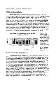
tromigration. As a consequence of the drive toward higher device AlCu densities the metallization lines interconnecting the devices on a chip 50 100 15 200 0 Number of voids (1/mm) already have dimensions (width and thickness) well below 1 pm. Fig.1 The number of voids per millimeter At the same time the push for faline length for 1 #m wide AICu and Alster circuits increases the current SiCu alloys deposited on SiO 2 or on TiW 2000C at stressed were Samples underlayers. densities in these lines. for 1 day. Stress-induced voiding was first identified some ten years ago [1,2] as line failures and voids appeared in interconnect lines at zero current density. The problem was soon identified to be caused by mechanical stress. During processing the patterned Al-alloy line is covered with an intermetal dielectric layer and/or a protective passivation layer. During the deposition the wafer is at a temperature of several hundred degrees centigrade, and the metal line will expa
Data Loading...