Thermal stability, microstructure, and electrical properties of atomic layer deposited Hf 6 Ta 2 O 17 gate dielectrics
- PDF / 861,132 Bytes
- 7 Pages / 585 x 783 pts Page_size
- 104 Downloads / 343 Views
Z. Yu, R. Gregory, K. Moore, P. Fejes, and S. Schauer Wireless and Packaging Systems Laboratory (WPSL), Freescale Semiconductor Inc., Phoenix, Arizona 85284 (Received 28 February 2007; accepted 21 June 2007)
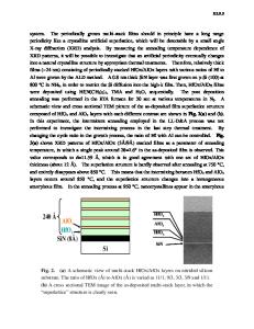
The intent of this work is to investigate thermal stability, microstructure, and electrical properties of thin Hf6Ta2O17 high-k gate dielectrics. X-ray diffraction and transmission electron microscopy analysis reveal that an as-deposited Hf6Ta2O17 film is amorphous with a ∼1-nm interfacial layer. After a 1000 °C anneal, the film is a mixture of orthorhombic-Hf6Ta2O17 and monoclinic HfO2 with a thicker interfacial layer. Uniform Hf and Ta Auger depth profiles are observed for as deposited and annealed films. Secondary ion mass spectrometry (SIMS) analysis shows Hf and Ta profiles are unchanged following the 1000 °C anneal, indicating good thermal stability. There is, however, a clear indication of Si up-diffusion into Hf6Ta2O17, particularly after annealing at 1000 °C. No Hf or Ta is found in the Si substrate. Well-behaved capacitance-voltage curves and low leakage current characteristics were obtained for Mo/ Hf6Ta2O17 capacitors for as-deposited and 1000 °C annealed films. A flatband voltage (Vfb) shift towards negative voltage is observed for the annealed film when compared to the as-deposited film, indicating the presence of more positive charge, or less negative charge. Furthermore, capacitance-voltage stress measurements were performed to study charge trapping behaviors. A smaller Vfb shift is observed for as deposited (
Data Loading...


