Three-DimensionalWafer Process Model for Nanotopography
- PDF / 809,315 Bytes
- 6 Pages / 612 x 792 pts (letter) Page_size
- 51 Downloads / 317 Views
F1.1.1
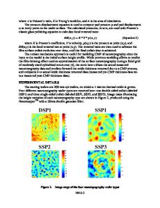
Three-Dimensional Wafer Process Model for Nanotopography Takafumi Yoshida YNT-jp.Com 2-10-17 Asae, Hikari, Yamaguchi 743-0021, Japan ABSTRACT This paper proposes a three-dimensional wafer process model for nanotopography. This model allows us to predict the effect and behavior of nanotopography on the wafer processes especially for the wafer Mechanical/Chemical Lapping (MLP/CLP), wafer Single/Double Side Polishing (SSP/DSP) and device Chemical Mechanical Polishing (CMP). INTRODUCTION Nanotopography of the wafer front side is becoming very important for the Shallow Trench Isolation (STI) CMP process [1]. To realize the high performance and high yield of device, IC makers have to optimize their CMP by taking into account the characteristics of nanotopography induced by silicon wafer makers’ processes [2]. An ideal silicon wafer process for nanotopography is exemplified in Figure 1. This example clarifies the importance of generating a crystallographic flat surface before slicing the silicon crystal ingot. This surface is to be used as a reference plane in the following wafer process to improve the nanotopography. However, this quality-oriented process is too expensive for silicon wafer makers to invest under today’s excessive low-price-competition circumstances. The conventional process is shown in Figure 2 with the features of the nanotopography and TTV (total thickness variation). Many silicon wafer makers have adopted the multi wire saw as their slicing technology on a cost-oriented policy. The wafer shape after slicing is modified by the following lapping process and then the etching process for the damage removal adds the roughness/waviness to it. Finally, the wafer shape is transmitted to various surface topographies according to the following polishing process such as SSP or DSP. The feature of the nanotopography after SSP heavily depends upon the mounting system such as a thin wax mount, thick wax mount or waxless (flexible) mount systems. In this paper, we propose a three-dimensional wafer process model for nanotopography to elucidate the behavior and to help to optimize CMP process for efficient planarization. Silicon Crystal Ingot
Damage Layer
Block Wax
Pad Flat Surface Grinding & ID Saw
Beveling
Wax Block
Grinding
Wax Mount
Mechanical/Chemical Lapping
Edge Polishing
Wax Mount
Mechanical/Chemical Lapping
Demount
Final CMP Chemical Cleaning Donor Killer Anneal /Epitaxial Growth
Figure 1. An ideal silicon wafer process for nanotopography
Downloaded from https://www.cambridge.org/core. Access paid by the UCSB Libraries, on 28 Oct 2019 at 08:46:14, subject to the Cambridge Core terms of use, available at https://www.cambridge.org/core/terms. https://doi.org/10.1557/PROC-767-F1.1
F1.1.2
Multi Wire Saw Platen
Block
Wax
Pad
or
Mechanical Lapping
Etching
Single Side Polishing with Thin Wax Mount
Single Side Polishing with Thick Wax Mount
Single Side Polishing Pad Double Side Polishing Wax Mount / Waxless
Single Side Polishing with Waxless Mount
Double Side Polishing
Nanotopogra
Data Loading...