Transistor Biasing
Active devices pose a design challenge due to their non-linear voltage–current characteristics. Inherently, there are two very different resistances that are found at each point of the V–I transfer characteristics, one static and one dynamic. When fixed v
- PDF / 641,281 Bytes
- 21 Pages / 504.581 x 719.997 pts Page_size
- 30 Downloads / 389 Views
Transistor Biasing
Active devices pose a design challenge due to their non-linear voltage–current characteristics. Inherently, there are two very different resistances that are found at each point of the V–I transfer characteristics, one static and one dynamic. When fixed voltage/current stimulus is applied at the terminals of an active device then by Ohm’s law we find static (i.e. DC) resistance at the given point simply by calculating V/I ratio. However, when the input signal varies relative to its average level, resistance to that change is then calculated by using the first derivative mathematical operation. Depending on the specific shape of a non-linear function, this dynamic (i.e. AC) resistance is very much dependent on the function’s curvature at the given static point, that is to say on its derivative. In this section we review basic technique to choose and setup DC and AC resistances of active devices, in a process known as the biasing setup.
5.1
The Biasing Problem
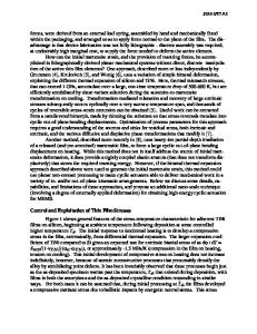
Fundamentally, a BJT device behaves as a current controlled current source, where the output current at collector is controlled by the input current at the base terminal through iC = β iB relationship, where β is the current gain of the device. In addition, a BJT is used as gm amplifier, that is to say, for the given input voltage vBE it delivers the output current iC . Unfortunately, our manufacturing technology is not ideal and, therefore, there are at least three main problems relevant to circuit design: (a) first, a BJT current gain factor β is not constant, it depends on both device geometry and on the manufacturing parameters. Unavoidably, the two have certain processing variations, which leads to the large variations of current factor β around its nominal value. What is more, β has strong temperature dependance and to a certain extent dependance on the collector current. The final consequence is that the overall realistic gain, which is expected to be fixed, if left uncorrected would have large variations, thus would render BJT devices practically useless. (b) second consequence is that gm also depends on collector current as well as on temperature. Detailed device analysis shows that base–emitter voltage VBE changes at the rate of 2.5 mV/◦ C. On the other hand, high-reliability electronic circuits must satisfy, for example, military and space standard which is specified within the environmental temperature range of T1 = −55 ◦ C to T2 =
© Springer Nature Switzerland AG 2021 R. Sobot, Wireless Communication Electronics, https://doi.org/10.1007/978-3-030-48630-3_5
157
158
5 Transistor Biasing
+125 ◦ C. Unavoidably, this wide temperature range of ΔT = T2 − T1 = 180 ◦ C causes the biasing VBE voltage to change by ΔVBE = 180 ◦ C × 2.5 mV/◦ C = 450 mV. At the same time, thermal voltage VT changes as VT (T2 ) =
kT2 = 34.31 mV q
VT (T1 ) =
and
kT2 = 18.8 mV q
As a consequence, taking a typical BJT transistor with (for example) VBE (T2 ) = 0.925 mV and VBE (T1 ) = 0.475 mV, while assuming constant saturation current IS , leads in
Data Loading...