Ultra High Vacuum Scanning Tunneling Microscopy Observation of Multilayer Step Structure on GaAs and AlAs Vicinal Surfac
- PDF / 1,762,820 Bytes
- 6 Pages / 414.72 x 648 pts Page_size
- 36 Downloads / 210 Views
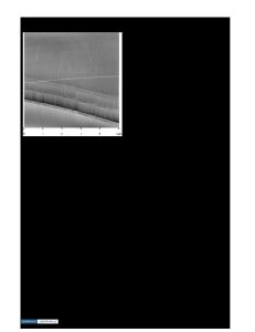
period superlattice, 60nm-thick GaAs layer, 15nm-thick Si doped GaAs conductive layer and 5nmthick non-doped GaAs top layer were grown at 600°C for GaAs surface observation, schematically shown in Fig. 1(a). In order to observe non-doped GaAs vicinal surface by UHV-STM, Si doped GaAs layer was inserted near the surface. For AlAs surface observation, I monolayer (ML) AlAs was also grown on GaAs top layer at 600 C. (Fig. l(b)). For AlAs sample grown at 700 C, the growth interruption was introduced at AlAs/GaAs interface during increasing the temperature. After the growth, the samples were transferred from the reactor to the RHEED chamber. For both GaAs and AlAs surfaces, c(4x4) reconstruction were observed by RHEED. Next, sample surfaces were passivated by amorphous As using Knudsen cell within RHEED chamber. The samples were loaded out from MOVPE system, and were loaded into UHV analysis system having UHV-STM chamber and X-ray photoelectron spectroscopy (XPS) chamber. Amorphous As on the sample surface was removed by heating in UHV analysis system. (a) (b) Oxidation free surfaces AlAs were confirmed by XPS 5nm GaAs measurement. UHV-STM 15nm n-GaAs images were observed under 60nm GaAs the negatively biased AlAs/GaAs SL condition for sample to tungsten tip which was held 100nm GaAs at ground potential (filled I Sub. II Sub. I images). The bias voltages were between -2 and -3 V, Fig.1 Schematic illustration of sample structures for (a) at constant current mode of GaAs surface observation and (b) AlAs surface 0.15 and 0.30 nA. observation. 3.Results and discussion First, UHV-STM image for GaAs vicinal surface is shown in Fig.2 (a). GaAs surface grown at 600 C has multilayer steps and atomically flat terraces. Average distance between each multilayer step is about 70nm, and the terrace region has no island. At the multilayer step region, 6 - 10 ML steps were bunched together, and (4x3) or (4x2) reconstruction units were observed between neighboring monolayer steps. [4] On this GaAs surface with multilayer steps, 1 ML -thick AlAs layer was grown at 600 or 700oC. AlAs surface grown at the temperature of 600 C has two dimensional nucleation on the 10 -2 terrace region, shown in Fig.2 (b). Island density on the terrace region is about 3x10 cm , and the average island separation is about 30nm. Because the two dimensional nucleation is only formed when AlAs layer grows on GaAs vicinal surface, these nucleation are composed of AlAs. The reason that the two dimensional nucleation is formed on terrace is that the distance between each multilayer step is larger than the migration distance of Al adatom. In previous works for GaAs growth on vicinal surfaces, we clarified from experiment [5] and simulation [3] that the distance between each multilayer step is limited by the migration distance of adatom. On the other hand, AlAs surface grown on GaAs vicinal surface at the temperature of 700°C has no island on the terrace region, shown in Fig.2 (c). These results suggest that the surface migration length of Al adatom increases with in
Data Loading...


