Ultra Shallow Junction Formation by B+/BF2+ Implantation at Energy of 0.5 KEV
- PDF / 1,151,906 Bytes
- 4 Pages / 417.6 x 639 pts Page_size
- 82 Downloads / 336 Views
1021
E
19
to10,
o
0
19I
10 is~
S10 18 17i
. 50
.ll1 100 Depth (rnm)
,
101. 1 150
0
200
a-Si
-s
010 10
a-Si
107 10 16 0
B* 0.5 kev
1020
6 kev
10B*
E '1
. . . . . .
'l8. 50
100 Depth (nm)
150
200
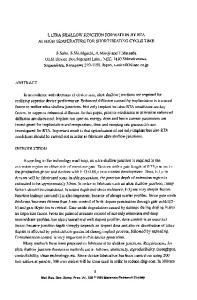
Figure 1. SIMS profiles showing the channeling tail dependence on B implant energy. B implants at 0.5 keV with l×X014 cm" 2 and at 6 keV with Ix1015 cm-2 . The shallower profiles for each energy are Ge-amorphized samples denoted a-Si in the graph. 13 Mat. Res. Soc. Symp. Proc. Vol. 532 © 1998 Materials Research Society
6
1000
6keV
6keV
5
600
6kUe
.s
40600k
0U-2
01
•
"0 12
200 0
13
14
15
16
12
Loglo(dose)
13
14
15
16
Loglo(dose)
Figure 2. Amount of channeling tail as a function of
Figure 3. Thermal wave unit as a function of implant
implant dose. Solid squares and circle indicate B
dose for B implanted into crystal Si.
implanted samples at 0.5 keV and 6 keV, respectively. Amount of channeling tail is defined as dose of channeling tail divided by total dose.
RESULTS Figure 1 shows depth profiles of B implanted at 0.5 keV and 6 keV into crystal and preamorphized Si. The 0.5 keV profile is shallower and has a much reduced channeling tail. Figures 2 and 3 show the amount of channeling tail and thermal wave (TW) respectively, as a function of the implant dose. In general, lower TW values mean lower damage, so larger channeling tail occurs. The 0.5 keV implanted sample, however, has low damage and a reduced channeling tail simultaneously. Figure 4 is a cross-sectional high resolution transmission electron microscope (HRTEM) image of the sample implanted with B at 0.5 keV with lxl015 cm"2. A highly damaged layer localized at shallower than 7 nm is observed. This suppresses the channeling tail with the low value of TW. The sample of 1xI03 cm2 , however, has a comparable channeling tail with 6 keV. Figure 5 shows depth profiles of B implanted at 0.5 keV into the crystal and preamorphized Si after RTA. The crystalline sample shows ajunction depth of 31 nm, that is defined as the depth at a B concentration of 2x1017 cm"3. The profile of the Gepreamorphized sample becomes deep due to TED. Figure 6 shows depth profiles of BF2 implanted at 0.5 keV into crystal Si, before and after RTA. The junction depth after RTA is 19 nm and TED is not observed. Figure 7 summarizes the diffusion length for the various implant conditions. The Ge-preamorphized samples have larger diffusion lengths. Because the B+or BF2+ is implanted into the amorphous Figure 4. Cross-sectional HRTEM image of Si
layer, the damage from the B or BF 2 implant does not dominate in the substrate. Likewise,
substrate implanted B at an energy of 0.5 keV with a dose of lx l0t5 cm 2 .
in the case of implantation in crystal-Si, TED 14
E
o 0
1021
1021
1020
1020
E
1019
1019 0 4) 0 V
8
1018
8. 1017
1017
1016 20
40
1016
60
0
Depth (nm)
20
40
60
Depth (nm)
Figure 5. SIMS profile of B implanted 0.5 keV after RTA.
Figure 6. SIMS profiles of 0.5 keV BF2 implanted sample before and after RTA.
is suppre
Data Loading...