Utilization of a-Si:H Switching Diodes for Signal Readout from a-Si:H Pixel Detectors
- PDF / 887,992 Bytes
- 6 Pages / 414.72 x 648 pts Page_size
- 1 Downloads / 279 Views
UTILIZATION OF a-Si:H SWITCHING DIODES FOR SIGNAL READOUT FROM a-Si:H PIXEL DETECTORS Gyuseong Cho, J.S. Drewery, W.S. Hong, T. Jing, H. Lee, S.N. Kaplan, A. Mireshghi, V. Perez-Mendez, and D. Wildermuth, Lawrence Berkeley Laboratory, Berkeley, CA, 94720
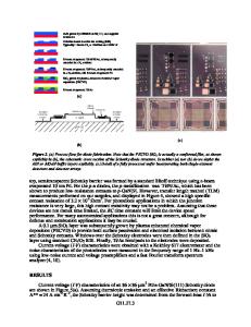
ABSTRACT Two-dimensional arrays of amorphous silicon photodiodes can be used as position-sensitive radiation detectors when they are coupled to an appropriate phosphor. We have developed signal readout schemes from amorphous silicon photodiode arrays utilizing one or two switching diodes attached to each pixel photodiode. Individual cells and prototype arrays of amorphous silicon photodiodes with single- and double-diode switching readout were fabricated and tested. A charge storage time and a readout time were measured. The measurement results were analyzed by simple circuit theory. INTRODUCTION Hydrogenated amorphous silicon(a-Si:H) diodes has been used for radiation detectors for X-rays, gamma rays and other charged particles.l1,2] Despite the poorer electronic characteristics of a-Si:H compared to crystalline silicon, it has the strong advantages of enabling the construction of large-area devices easily and inexpensively. Also it has been shown [31 that this material has a much higher radiationresistance compared to the crystalline material. Two-dimensional (pixel) arrays of photodiodes for X-ray imaging conventionally use a-Si:H TFTs as switching elements. Schematics of the array and the element are shown in Fig. 1. and Fig. 2. (a) [4] The signal charges generated by photons are first stored in each pixel detector capacitance during the first part of the scanning cycle. Then in the second part of the cycle, the stored charges are sent to an external multi-signal processor in a row through switching transistors when a gate pulse is applied sequentially. K. Yamamoto et al. [5] also have made 2-d image sensors using single-diode switches as a replacement for TFTs; its schematic is shown in Fig. 2 (b). TFT switching seems to be better for controlling the detector bias and in avoiding the cross-talk between pixels, but it requires a more complicated fabrication process including the additional deposition of a high quality gate dielectric layer(Si3N4 or SiO 2 ). Single-diode switching has the advantage that the switching diodes use the same p-i-n layers as the photodiode. Therefore the number of masks required in lithography will be reduced. However this method Mat. Res. Soc. Symp. Proc. Vol. 297. @1993 Materials Research Society
970
Switching
Bias Line .-----. 0
TFT .e
LBias Photodiotte
I
Gate Pulse
I
-~
0
Line * Line Signal Line l Signal ISignal Ln
Gae Pulse
1
TFT Out
Gate Pulses
Switching Diodes
+
Pixel
Detector
Signal Out
Signal Out
Multi-Signal Processing IC
S(a)
(b)
(c)
Fig. 1. Schematic diagram of a-Si:H pixel
Fig. 2. Realization of pixel switches with
detector array using TFT switches.
(a) TFT, (b)single- and (c) double-diode.
intrinsically possesses some problems such as a large switchingtransients as well as the uncontrollab
Data Loading...