Alloying Behavior and Reliabilty of Pt Embedded Metal/n + -GaAs Thin Ohmic Contact System
- PDF / 1,413,523 Bytes
- 6 Pages / 414.72 x 648 pts Page_size
- 66 Downloads / 275 Views
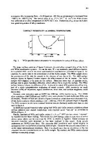
EXPERIMENTAL The 0.1 gin n+-GaAs layer was grown by metalorganic chemical vapor deposition on the semi-insulating (100) oriented GaAs substrates. Undoped buffer layer of I jIm thickness was deposited between these layers. Carrier concentration of the as-grown n+-GaAs layer was lxi018 cm- 3 . Prior to metal deposition by electron-beam evaporator, the wafers were etched in a solution of pure HF for 90 sec and rinsed in DI. water to remove any surface oxide. Transmission Line Method (TLM) pattern was made by photolithography. Prior to metal deposition the wafers were chemically cleaned again using a solution of HCI:H 2 0=1 :3 for I main. Fig. 1 illustrates schematic cross-section of the samples. Sample A has the configuration of AuGe(12at%-Ge)-800 A/Ni-150 A/ Pt-200 A/Au-500 A/ n'-GaAs. Sample B is identical to sample A except that the deposition order of Ni and Pt is reversed: AuGe-800 A/ Pt-200 A/Ni150 A/Au-500 A/n+-GaAs. For contact resistance and sheet resistance measurements, samples with TLM and van der Pauw patterns were prepared on the mesa etched n+-GaAs layer. Ohmic metal pad and dot line were also fabricated on mesa etched n'-GaAs by liftoff. Ohmic contact was obtained by rapid thermal annealing (RTA) for 10 sec at 430 IC in N2 ambient. Reliability test was carried out in N 2 ambient System A System B for 486 hr, 2500 hr, and 3000 hr at isothermal temperature of 300 1C. The metals adhered well Au-500 A Au-500 A to GaAs without peeling. Auger electron spectroscopy(AES) and XPt-2oo A ray diffraction(XRD) were utilized to measure Pt-2OOA Ni-15s A the interfacial reactions and to study the phases formed. Atomic force microscopy (AFM), AuGe-800 A Scanning electron microscopy(SEM), and AuGe-800 A transmission electron microscopy(TEM) were employed to examine the surface and interface Fig. 1Cros-sectin+aschaAs of samples Fig. 1. Cross-sectional schemes of samples morphology and microstructural changes. RESULTS Specific Contact Resistance 10
Fig. 2 shows the variation of specific contact resistance as a function of aging time for both systems. Minimum specific contact resistance is 7 2 9x10- QM c . This specific contact resistance is higher than that for AuGeNi scheme: 10-7-10-6 2 cm 2 for n--10 7 cm- 3 . But the characteristics of specific contact resistance showed nearly same even after thermal storage test for 3000 hr. Fig.2. Specific contact resistance variations as function of aging time. (The solid line is system A and the dotted system B).
390
"U 0
I
U
:x 10" (Qcm2)
f
--- AuGe/Ni/P/Au ...AuGe/Pt/Ni/Au
......... __T_
U) 0.:
0.1
RTA 500 1000 1500 2000 2500 3000 Aging Time (hr)
Phase Identification and Atomic Redistribution Fig. 3 presents XRD profiles for system A. The result of system B was identical except for the difference of intensity ratio of double peak(Au 7 Ga2) at 2 0 - 400. In the figure, XRD peaks corresponding to 83-Au7 Ga 2 (/3 -AuGa, hexagonal), PtAs2 (cubic), and Nil 9Ge 12 (hexagonal) were clearly observed. Furthermore, these phases remained unchanged even after a 3000-hr thermal s
Data Loading...