Backside Storage Non-Volatile Memories: Ultra-Thin Silicon Layer on a Complex Thin Film Structure
- PDF / 460,593 Bytes
- 5 Pages / 612 x 792 pts (letter) Page_size
- 94 Downloads / 334 Views
D1.4.1
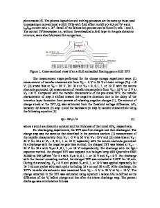
Backside Storage Non-Volatile Memories: Ultra-Thin Silicon Layer on a Complex Thin Film Structure H. Silva and S. Tiwari School of Applied and Engineering Physics, Cornell University, Ithaca NY 14853, USA ABSTRACT Backside storage memories present an alternative to the conventional front-floating gate geometries by storing charge in defects on the back of a thin depleted silicon channel. This paper focuses on the fabrication of these devices using a modified Smart-Cut™ substrate preparation process followed by standard CMOS processing. The substrate is a complex silicon-on-insulator (SOI) substrate where instead of the buried oxide alone a charge trapping multi-layer stack of oxide-nitride-oxide (ONO) is used as the buried insulator. We demonstrate here the operation of these device structures at ultra-short length scales and summarize the characteristics of their operation. INTRODUCTION The difficulties in making smaller silicon non-volatile memories with the conventional front-floating gate geometries arise from non-scalability of the gate stack (injection oxide, storage medium, and control oxide) as gate length is reduced. For high density and low power applications, the memory performance - retention and reliability – is inevitably compromised in the sub-70 nm dimension range. The backside trapping structure (Fig.1.) presents an alternative by storing charge in defects on the back of a thin depleted silicon channel. Charge trapped in the ONO stack causes a threshold voltage shift in the read transistor (front silicon interface). A very thin silicon body allows the scaling of the device to very short gate lengths and at the same time good coupling between the charge stored in the back and the front silicon interface (read transistor) for efficient memory operation. The device can be written using Fowler-Nordheim (FN) tunneling, by applying a large positive voltage to the back-gate while keeping front-gate, source and drain grounded, or by Hot Electron Injection (HEI), with a moderate positive back-gate voltage combined with a drain voltage in the order of 3.5-4 volts to create hot carriers. The device is erased by FN tunneling by applying a large negative voltage to the back-gate with the front terminals grounded. Decoupling the read from the write/erase functions in this structure allows the use of a thin read gate oxide to efficiently turn-off the device minimizing power dissipation in read/standby mode even at very short gate lengths and a thick write/erase gate stack to ensure good retention time and cycling endurance [2-5].
read gate oxide
Gate
tunneling oxide
storage medium
Back-Gate
control oxide
Figure 1. Schematic cross-section of a backside trapping memory.
D1.4.2
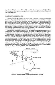
SUBSTRATE PREPARATION Fig. 2. illustrates the fabrication process sequence for these devices. The devices are fabricated using a modified ‘smart-cut’ substrate preparation process followed by standard CMOS processing. We start with two silicon wafers, a low doped p-type wafer, the donor wafer, and a highly doped n-type wafer,
Data Loading...