Characterization Techniques For Laser-Annealed Polysilicon on Insulating Layers
- PDF / 3,610,280 Bytes
- 8 Pages / 415.8 x 637.2 pts Page_size
- 25 Downloads / 278 Views
479
CHARACTERIZATION TECHNIQUES FOR LASER-ANNEALED POLYSILICON ON INSULATING LAYERS
J. T. SCHOTT Sperry Research Center, J. J. COMER RADC, Hanscom AFB,
Sudbury, Massachusetts
Massachusetts
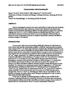
ABSTRACT Various characterization techniques are applied to pulsed and cw laser-annealed polysilicon layers deposited on oxide layers. The results are used to compare these techniques as to the type and completeness of information provided, as well as sample preparation requirements and general ease or difficulty of measurement. The techniques employed include scanning electron microscopy (SEM), electron channeling micrographs and selected area channeling patterns (SACP), reflection (high energy) electron diffraction (RHEED), transmission electron microscopy (TEM) and selected area diffraction (SAD), x-ray diffraction, optical techniques and etching techniques. I:TRODUCTION Laser annealing of polysilicon has potential application in two different areas of MOS device processing. For standard MOS/bulk technologies, ionimplanted polysilicon can be laser annealed to provide a high degree of dopant activation as well as large grain crystallization for low resistivity interconnects. Crystallization can also reduce the sensitivity of resistivity to dopant level for low dopant levels. Second, large grain crystallization of polysilicon layers on insulating layers offers the potential of producing device quality silicon-on-insulator structures for dielectric isolation as an alternative to silicon-on-sapphire. There is the further possibility of polysilicon crystallization on top of completed integrated circuit layers to provide true vertical integration for three-dimensional integrated circuits. In both of these areas, but particularly for silicon-on-insulator applications, a complete materials characterization of the crystallized poly layer is essential. Samples were prepared by LPCVD deposition of polysilicon of various thicknesses (0.25 lim-0.5 Vm) on various thicknesses of oxide (700 A - 1 Pm) on (100) single-crystal substrates. The poly was either doped (various As and P implant fluences) or undoped. Some samples received a pre-laser anneal heat treatment and some had an oxide covering over the poly. In some samples, the poly was patterned into islands before laser annealing. Laser annealing was performed on commercial systems which use either a cw argon ion laser or pulsed Nd:YAG laser, and the samples showed various degrees of crystallization up to large grains hundreds of micrometers long and single-crystal islands. Some of these results have been reported elsewhere [l]. CHARACTERIZATION TECHNIQUES Decoration etch. The simplest method to obtain information about the crystalline structure of laser-annealed poly films is with a decoration etch to delineate the grain boundaries. The Secco etch [2] has been used for this purpose [3] and works very well. A very brief etch (approximately 5 sec) sharply
480
Fig. 1. Optical micrograph (100OX) of cv laser annealed polysilicon on oxide following Secco etch.
Fig. 2. Optical micrograp
Data Loading...