Comparison of Heat-Pulse and Furnace Isothermal Anneals of Be Implanted InP
- PDF / 849,847 Bytes
- 6 Pages / 417.6 x 639 pts Page_size
- 97 Downloads / 252 Views
COMPARISON
OF HEAT-PULSE AND FURNACE ISOTHERMAL ANNEALS OF Be IMPLANTED InP
B. MOLNAR,* G. KELNER,* G.L. RAMSEYER,* G.H. MORRISON,** S. C. SHATAS,*** *Naval Research Laboratory, Washington, D.C. 20375; **Cornell University, Ithaca, N.Y. 14853; and ***AG Associates, Palo Alto, CA 94303 ABSTRACT Annealing in the 600-900*C temperature range, using either a halogen lamp for periods of seconds or a furnace for periods of minutes, has been applied to activate Be implanted InP samples. The Be was ion-implanted at room temperature into InP substrates. The substrates were uncapped and in close contact with another smooth surface during annealing. 17
19
3
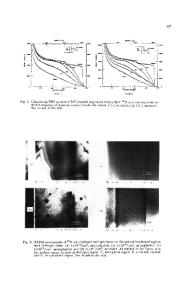
It was found that in the 10 -10 /cm range, the acceptor concentration increased with the temperature of anneal. It was also found that redistribution effects decreased with decreasing anneal time. For short anneals, the optimum condition for an 80-90% activation in the 10 1 7 -10 1 8 /cm 3 range was estimated to be 10 seconds at 950°C. It was also found that after rapid anneal, the carrier concentration profile closely approximated the as8 9 3 implanted Be profile. In the case of 101 -101 /cm implants, which were 16 7 3 rapidly annealed, there was a low concentration component (10 -101 /cm ) to the redistribution; this ancillary component to the main active distribution was detected by SIMS and was electrically inactive. For long term annealing this electrically inactive Be component was partly converted to substitutional Be and became electrically active. Rapid thermal annealing eliminated this conversion. INTRODUCTION The development of controllable acceptor doping of InP by ion implantation is important for several electronic device applications. Because it creates less damage than other heavier p-type ions, low mass Be is particularly attractive for p-layer formation. Be has already been used for p-n junction formation in InP diodes [1,2,31. Such devices require precise control of the impurity concentration. For furnace annealed cases, appreciable spreading of Be has been observed[4,51. During the past few years several short time anneal techniques [6] have been explored for annealing ion implantation damage while producing minimal dopant diffusion. Such techniques use a variety of energy sources and can thermally process materials in the 108-_102 s range. This is short compared to a standard 15-20 min thermal anneal. Annealing of ion implanted InP with pulsed laser beams [7], pulsed electron beams [8], and different lamps [9,10,111 has been successfully applied over a broad range of time. It has recently been demonstrated [111 18 3 that a few second lamp anneal of 10 /cm Be, results in dopant activation and mobilities comparable with the best furnace anneal. The lamp anneal technique is simple, relatively inexpensive, and minimizes the effect of thermal gradients. We have established [5] that for Be implantation at a level of 10 1 8 /cm 3 , or higher, a significant tail develops during the thermal anneal. The comparison of atomic (SIMS) and electronic (C-V) carrie
Data Loading...


