Critical Materials, Device Design, Performance and Reliability Issues in 4H-SiC Power Umosfet Structures
- PDF / 1,183,711 Bytes
- 6 Pages / 414.72 x 648 pts Page_size
- 69 Downloads / 313 Views
S
Ei+ =1.5 MV/cm
Noor P+doped Source
Polys licon gate
Iy
Source
N+4R-bSic 3.25
Drain
18nm
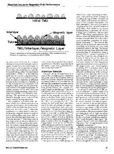
Energy band diagram of N+ 41Fig. 2 ISiC/SiO3Polysilicon system under on-condition
A schematic cross-section of a unit cell of the 4H-SiC UMOS showing all the active layers. In a Fig. 1
CK ....r
.[VV.
device, there are N cells each of width W and pitch S.
In order to study the FN tunneling, metal-oxide-semiconductor (MOS) capacitors were made on the silicon face of the p-type 4H1-SiC by pyrogenic oxidation at 1050°C for six hours followed
by 1 hr. anneal in Argon and 1.5 hr. anneal in oxygen at 9501C. Approximately 460
A of silicon
nitride was deposited on top of the thermal oxide and gold dots were evaporated. The backside A•of Al layer of the wafer was cleaned by reactive ion etching the oxide and the nitride and 5000 0
was thermally evaporated. Finally, the wafer was annealed in forming gas at 450 C for 1 Hr. FN tunneling measurements were made by stepping a positive bias on the top electrode, creating an inversion layer at each bias step by illuminating with a UV source for 1 minute, and then 3. The composite insulator measuring the current in the dark. The results are shownin tFig. breaks down at about 11-12 MV/cm electric field at room temperature and about 5 MV/cm at 325°C. The FN plots indicate much higher current density at a given field in SiC as compared to silicon. The current density in SiC increases much more rapidly with temperature as compared to silicon indicating the presence of enhanced thermionic field emission due to lower barrier in SiC/SiO2 system.
Electric Field in the Gate Insulator Under Off-Condition The electric field in the insulator over the bottom corner of the trench, El_, under off condition
with maximum voltage on the drain should not exceed about 2 MV/cm to avoid FN tunneling of electrons from the conduction band of N+ ploysilicon gate into the insulator at room temperature. This limit may be raised to about 3 MV/cm if Pc doped polysilicon gate is employed due to about I V increase in the barrier (Fig. 4) [5]. A 2-D simulation using MEDICI software from TMA indicates the field crowding in the insulator near the bottom corner. Taking into account the and SiC (3.9/10), the maximum field in SiC at the SiC/Sin 2 ratio of dielectric constants of 2 eiO interface in the bottom flat region of the trench should not exceed about 0.75 MV/cm. Assuming some charge sharing with the adjacent channel [6], this limit may be raised to about 1 MV/cm at room temperature. Again, this limit should be lowered at elevated temperatures. As the breakdown field of 4b -SiC is about 3 MV/cm, it is clear that in devices such as UMOS or IGBT where gate insulator is subject to the high field stress under off-condition, the design and performance is limited by the insulator reliability issues rather than intrinsic SiC properties. These reliability issues become more severe at elevated temperatures and thus it is difficult take
88
advantage of low leakage currents operating high at in SiC temperatures. T
Data Loading...