Crystallographic Texture Characterization of Inlaid Copper Interconnects
- PDF / 788,403 Bytes
- 6 Pages / 612 x 792 pts (letter) Page_size
- 10 Downloads / 501 Views
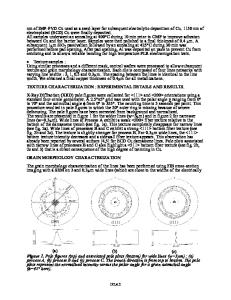
CRYSTALLOGRAPHIC TEXTURE CHARACTERIZATION OF INLAID COPPER INTERCONNECTS Inka Zienert,@ Paul Besser,# Werner Blum,@ and Ehrenfried Zschech@ @ Materials Analysis Department, AMD Saxony Manufacturing Dresden, Germany # Technology Development Group, Advanced Micro Devices, Sunnyvale, CA, USA INTRODUCTION Developing faster integrated circuits places incredible demands on the interconnect system. The smaller feature sizes lead to excessive current densities, which in turn make the interconnect lines more susceptible to electromigration (EM) failure.[1] Studies have shown that EM performance can be improved by increasing the strength of the {111} texture in conventionallyfabricated aluminum-based lines.[2-6] The strong {111} texture minimizes the presence of highangle grain boundaries along the interconnect line, thus minimizing a fast-diffusion path for EM mass transport.[2-4,7-12] As the integrated circuit industry is replacing Al with the more EM resistant Cu,[12-27] the role of texture in improving Cu reliability and integration is an important concern. The texture in the Cu interconnects is more complicated than that for Al, since the Cu lines are fabricated using inlaid methods rather than deposition and subtractive etch methods. Sidewall-oriented grains are expected and have been observed, [16-21] being more prevalent in narrow lines.[17-21] Studies to correlate microstructure,[22-25] in particular, texture[17,25] to EM have been conducted with inlaid Cu lines. These and other studies have shown that interface diffusion is the dominant diffusion mechanism leading to EM failure.[23,26,27] However, when the interface diffusion is reduced, texture will need to be improved for Cu as it was for Al. Another reason to quantify the texture is that the grain growth and orientation of the Cu grains affect the integration of Cu in inlaid lines. Some authors have observed that, during annealing of inlaid lines prior to CMP, Cu grains grow from the overburden into the trenches,[19,20] while others observe that grain growth occurs independently of the overburden.[17] Texture measurements are a valuable tool for understanding grain growth in trenches. EXPERIMENTAL Dual inlaid Cu lines were produced using an abbreviated version of a logic technology flow. Inlaid Cu lines were fabricated in the interlayer dielectric (ILD) using an oxide patterning and etch technique. The 4.5 kÅ deep trenches had 85° sidewalls. Following deposition of a barrier and Cu seed, the 0.35 µm wide trenches were completely filled with electroplated copper using a commercially available electroplating tool. Chemical mechanical polishing (CMP) was used to remove excess Cu and electrically isolate the lines, and a SiNx/oxide capping layer deposited. In contrast to unpatterned copper films, grains in inlaid structures nucleate and grown from the bottom and the sidewall of the trenches. Therefore arrays of lines give more realistic results.[1720,28-29] Crystallographic orientation of the Cu grains in the lines can be quantified with X-Ray diffraction (XRD) or El
Data Loading...