Directions in the Chemical Mechanical Planarization Research
- PDF / 542,175 Bytes
- 9 Pages / 420.48 x 639 pts Page_size
- 12 Downloads / 396 Views
INTRODUCTION
The planarization, achieved by the use of chemical mechanical means, has enabled the interconnection of ever increasing number of devices and also the use of lower resistivity copper as the interconnect material for such devices. The effectiveness of the chemical mechanical planarization (CMP) (1)in both improving the yield and performance of the circuits has let to its' application in the front end processes and many other microelectronic applications (in both
advanced and not-so advanced devices and circuits). This tremendous growth of CMP applications is largely associated with the clever engineering developments and solutions generally credited to the tool and consumable providers. It has led many of us to believe that there are no showstoppers. However, as the technologies move (a) from sub-0.25jim minimum feature size (mfs) regime into the sub-0.10 jim mfs regime and multi-layered structures and (b) into the three-dimensional (3D) structures, CMP will face new challenges. In the sub-0.10 pjm regime of the devices, atomically flat and clean surfaces will be needed. This is true for both today's silicon based devices and new devises that have not yet been developed or found a competing edge over existing ones. For example, atomically flat and clean silicon surfaces have been oxidized to produce near-nm-thick gate oxides for the metal-oxide-semiconductor (MOS) device fabrication. (2)These MOS devices, employing polysilicon as the metal, have been shown to work with leakage currents that are a function of the atomic flatness at the Si-Si0 2 interface, increasing with increasing roughness. Note that the art of the preparation of such atomically smooth surfaces is known to mankind in both the semiconductor and optics industry. The use of the so-called chemical mechanical polishing (many a time used as acronym in place of CMP) and controlled vapor disposition techniques have been made in producing the desired atomic smoothness of the surfaces. The challenges that lie ahead refer not only to the preparation but
Mat. Res. Soc. Symp. Proc. Vol. 566 ©2000 Materials Research Society
also to preserving such atomically smooth large area surfaces before, during, and after the next step in the process of fabricating semiconductor devices/circuits. In many circumstances such preparations will cover the use of large-area and multi-material (single or polycrystalline) surfaces with the unprecedented planarity requirements. In spite of the so-called no showstopper attitude, it is obvious that there remain (a) a large number of nuances and effects listed in Tables 1 & 2 and (b) a lack of fundamental understanding that need to be addressed and evaluated for the continued success of CMP into the sub-tenth micron era. Added to these challenges, and as suggested above, will be the introduction of new metals (Cu, Cu-alloys, diffusion barrier/adhesion/ promoters), new interlayer dielectrics (ILD) (polymers, aero/xerogels. others), high dielectric constant materials, and optoelectronic materials. Stringent control on t
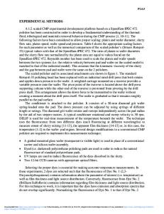
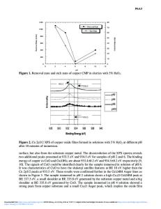
Data Loading...