Metrology Issues in Cu-Low-K Chemical Mechanical Planarization
- PDF / 604,275 Bytes
- 6 Pages / 612 x 792 pts (letter) Page_size
- 80 Downloads / 478 Views
Y9.7.1
METROLOGY ISSUES IN CU-LOW-K CHEMICAL MECHANICAL PLANARIZATION Parshuram B. Zantyea,b, Arun K. Sikderb, Swetha Thagellab, Nivedita Gulatia,b and Ashok Kumara,b a Department of Mechanical Engineering, b Center for Microelectronics Research, University of South Florida, Tampa, FL 33620
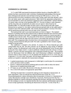
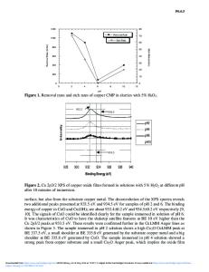
Abstract Ultra low-k materials used in Cu damascene process are inherently soft and weak in nature; hence the evaluation of tribological properties of these materials is an issue of paramount importance in the field of semiconductor fabrication. Chemical Mechanical Polishing (CMP) of these films is a major challenge due to their reduced modulus and cohesive strength. The objective of this research is to develop a strong understanding of the tribological properties of Cu ultra low-k dielectric materials for successful implementation in the semiconductor devices. The Cu ultra low-k systems are polished at different conditions of load and platen rotation and their polishing behavior is compared with the standard Cu-SiO2 system. The polishing behavior of Cu and the barrier Ta material is studied in order to effectively detect the end point of the Cu CMP process. Delamination studies, post process surface characterization using scanning electron microscopy and the reliability issues of these materials also come within the scope of this study.
Introduction With the progressive decrease in the feature size, the interconnect delay measured by RC (Resistance X Capacitance) of a circuit increases non-linearly and is much larger than the delay in switching the transistor (gate delay) [1]. For the feature size of 180 nm (present generation technology), the interconnect delay is the rate limiting factor for faster devices [2]. To counter the adverse effect of RC time delay, new multilevel metallization (MLM) schemes, which span several planes and are isolated by dielectric insulating layers, have been developed. Presently schemes with up to 6-8 metal layers have been developed to counter the adverse effects of RC delay. Concomitantly, to further reduce the RC delay and decrease the number of levels, low resistivity materials such as copper and low dielectric constant materials such as fluorinated silica, carbon and polymers can be used [3]. It is estimated that by using low-k dielectric polymeric materials and copper, the number of metallization multilevel can be reduced from 12 to 6 for 0.13 µm devices [4]. The problems associated with MLM structures are all related to deposition, alignments (lithography, patterning and etching), planarization, etc. The CMP process offers a lot of versatility, simplicity and better global planarization and can be applied for planarization of all type of materials [5]. Besides addressing the need for global planarization, the CMP process is the only method for making patterning lines of materials such as copper, which is difficult to etch and pattern by conventional dry etching methods [5]. This method known as the ‘damascene’ or inlaid approach’ deposits blanket copper on silica which has been patterned w
Data Loading...