Electromigration of Cu Interconnect Lines Prepared by a Plasma-based Etch Process
- PDF / 2,291,984 Bytes
- 6 Pages / 612 x 792 pts (letter) Page_size
- 24 Downloads / 371 Views
1079-N09-02
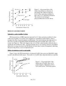
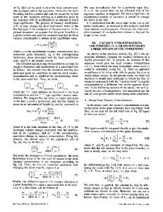
Electromigration of Cu Interconnect Lines Prepared by a Plasma-based Etch Process Guojun Liu, and Yue Kuo Texas A&M University, Thin Film Nano & Microelectronics Research Laboratory, 235 J. E. Brown Engineering Bldg., MS 3122, College Station, TX, 77843-3122 ABSTRACT The electromigration performance of Cu lines patterned by a Cl2 plasma-based etch process has been studied with the accelerated isothermal lifetime test. An electromigration activation energy of 0.6 eV and a current density acceleration exponent of 2.7 were obtained. Both the copper-silicon nitride cap layer interface and the copper grain boundary were active diffusion paths. The applied mechanical bending stress changed the electromigration void distribution in the film, which leaded to the shorter lifetime and lower activation energy. INTRODUCTION Electromigration (EM) is one of the most critical reliability issues for modern ultra large scale integrated (ULSI) circuits due to the aggressive decrease of interconnect dimension and the subsequent very large current density [1]. Copper (Cu) interconnects are typically patterned by a damascene process, using the chemical mechanical polishing method to remove the Cu film outside of the dielectric trench. Recently, Kuo and Lee reported a new plasma-based Cu etch process [2, 3]. Instead of vaporizing the plasma/Cu reaction product formed in Cl- or Br-based plasma exposure, a dilute hydrogen chloride solution was used to dissolve the reaction product of CuClx or CuBrx. EM studies on the damascene Cu line showed that it had a lifetime one or two orders of magnitude longer than that of the aluminum (Al) line.[1] However, the EM performance of the Cu lines patterned by the plasma-based etch process has not been explored. The EM induced failure occurs due to the flux divergence. Microscopic divergence can happen at a triple junction point of the grain-boundary network or any other location where the inhomogenous mass transport occurs [4]. Macroscopic divergence may occur at the bottom of via for the two-level testing structure where the via or the barrier layer blocks the EM flux, or the interface between Cu and the cap layer where the interfacial diffusion is the primary transport mechanism [5]. It is necessary to identify the diffusion path and to determine the activation energy (Ea) of the EM failure process before the Cu line’s reliability can be understood. Previously, a wide range of Ea values were reported due to different diffusion mechanisms. For example, the lattice diffusion corresponded to an Ea value of 2.1 eV and the grain boundary diffusion showed an Ea value of 1.2 eV [6]. For Cu metallization, the surface or interface diffusion is often the primary failure mechanism. Proost reported the Ea value of 1.06 eV for the Cu-metal interface diffusion [7]. An Ea value between 0.6 and 0.88 eV was reported on the Cudielectric interface diffusion mechanism [8]. The EM performance depends not only on the film structure, but also the patterning process. Fillipi et al. compared the EM tests of the
Data Loading...