Environmental Impacts of Crystalline Silicon Photovoltaic Module Production
- PDF / 103,008 Bytes
- 9 Pages / 612 x 792 pts (letter) Page_size
- 73 Downloads / 390 Views
0895-G03-05.1
ENVIRONMENTAL IMPACTS OF CRYSTALLINE SILICON PHOTOVOLTAIC MODULE PRODUCTION Erik A. Alsema1 and Mariska J. de Wild-Scholten2 1 Copernicus Institute of Sustainable Development and Innovation, Utrecht University, The Netherlands, e-mail: [email protected]; 2 Energy research Centre of the Netherlands (ECN), Petten, The Netherlands, e-mail: [email protected].
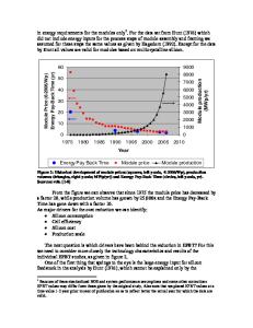
ABSTRACT: Together with a number of PV companies an extensive effort has been made to collect Life Cycle Inventory data that represents the current status of production technology for crystalline silicon modules. The new data cover all processes from silicon feedstock production to cell and module manufacturing. All commercial wafer technologies are covered, that is multiand monocrystalline wafers as well as ribbon technology. The presented data should be representative for the technology status in 2004, although for monocrystalline Si crystallisation further improvement of the data quality is recommended. On the basis of the new data it is shown that c-Si PV systems are in a good position to compete with other energy technologies. Energy Pay-Back Times of 1.7-2.7 yr are found for South-European locations, while life-cycle CO2 emissions are in the 30-46 g/kWh range. Clear perspectives exist for further improvements of roughly 40-50%.
INTRODUCTION Reliable data on the environmental impacts of PV module manufacturing have been rather scarce for the last 10-15 years. The only extensive data collection based on production data were published in 1992 [1] and were based on technology from the late 80’s. Later work was done to update these data but this was to a large extent based on secondary data sources and estimates [2, 3, 4]. Consequently, life cycle assessment and external cost studies were often based on the old data set that do not really reflect the technological progress made over the past decade. In a unique collaboration with 11 PV companies from Europe and the USA, we have improved this situation. The contributing companies together cover the complete production chain for crystalline silicon PV modules, from poly-silicon production to module assembly. Also they cover all three major technologies for c-Si, namely multicrystalline, monocrystalline and ribbon silicon wafer technology. This effort was conducted in the framework of the CrystalClear project, a large European Commission co-funded Integrated Project focusing on crystalline silicon technology. In this paper we present the results of a Life Cycle Assessment study on the basis of these new data. DATA COLLECTION The data collection and processing is fully described in a separate paper [5], so we mention here only the main characteristics. All data were collected in the period September 2004 –
0895-G03-05.2
November 2005 and are representative for the technology status in 2004. Cell production data for the considered facilities totalled about 160 MWp in 2004, all of them located in Europe. Also for multi-Si wafer production we cover a sizable share of the European market, while for r
Data Loading...