Evolution Of Defects Induced By High Energy He Implantation In Gold-Diffused Silicon
- PDF / 237,260 Bytes
- 7 Pages / 595 x 842 pts (A4) Page_size
- 13 Downloads / 360 Views
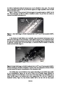
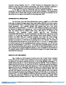
Evolution Of Defects Induced By High Energy He Implantation In Gold-Diffused Silicon R. El Bouayadi, G. Regula, B. Pichaud, M. Lancin, J. J. Simon, E. Ntsoenzok 1 Laboratoire TECSEN, Aix-Marseille III, Service 151, Marseille, F-13397 1 CERI-CNRS, 3A, rue de la Férollerie, Orléans cedex, F-45071 ABSTRACT Silicon samples were gold-diffused at different temperatures, implanted with He ions at 1.6 MeV and then annealed at 1050°C for 2 hours. The implantation induced-defect structure and their distribution in the depth of the sample, studied by conventional and high resolution cross section electron microscopy (HRXTEM) depend on the gold level introduced in the wafer prior to the gettering process. A high concentration of gold in silicon seems to influence the defect configuration in the cavity zone. Indeed, gold chemisorbed at cavities can homogenize the surface energy of their planes in different orientations, and can increase the cavity critical diameter beyond they become facetted. Secondary ion mass spectroscopy (SIMS) profiles exhibit a shouldered shape and a width closely related to the presence of the defects (observed by XTEM) which are very efficient sinks both for gold and copper atoms. Unfortunately, the electrical improvement of the material (checked by minority carriers diffusion length measurements MCDL) is not achieved by this gettering process, probably due to the high metal impurity concentrations remaining out of the gettering zone, to the presence of AuCu complexes and η-Cu3Si precipitates identified by deep level transient spectroscopy (DLTS) measurements and HRXTEM observations respectively. INTRODUCTION Metal impurities are known to degrade dramatically the performances of silicon based devices even in concentration as low as 1012 at.cm-3 [1]. Dissolved in the silicon bulk, these impurities can strongly reduce the minority carrier diffusion length. With the size reduction of the device structure, it is more and more interesting to create very localised gettering zones at, or just below, the active zone. This so-called proximity gettering have been carried out in Si [3,4] by implantation of different kind of ions (C+, Si+ etc…) but there is also a great deal of interest in He or H implantation [5-7]. In silicon, He and H segregate into small gas-vacancy complexes which favor bubbles or cavity formation depending on the implantation and on the subsequent heat treatment conditions [8]. The gettering ability of such cavities have been demonstrated for transition metals at keV energies [6-9] but only few work has been carried out at MeV energies [10]. In this study, in the latter energy range of He implantation, we have investigated the cavities (and implantation related defects) and we have checked their gettering efficiency for Au and Cu atoms by two means: i) chemically by SIMS measurements and ii) physically by showing a nanostructure change of the cavities in highly gold-doped samples. Moreover, this combination of metal impurities is interesting because each metal diffuses in a different way in si
Data Loading...