Silver Nanocrystals at Cavities Created by High Energy Helium Implantation in Bulk Silicon
- PDF / 2,314,414 Bytes
- 6 Pages / 595 x 842 pts (A4) Page_size
- 114 Downloads / 315 Views
0994-F11-06
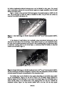
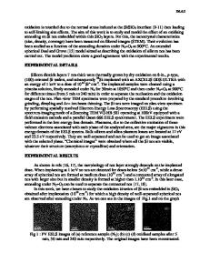
Silver Nanocrystals at Cavities Created by High Energy Helium Implantation in Bulk Silicon Rachid El Bouayadi1, Gabrielle Regula2, Maryse Lancin2, Eduardo Larios3, Bernard Pichaud2, and Esidor Ntsoenzok4 1 LES, University of Oujda, FacultÈ des sciences, B.P. 717, Oujda, 60000, Morocco 2 TECSEN, Paul CÈzanne University, Aix-Marseille III, Avenue de l'Escadrille Normandie Niemen, Marseille, 13397, France 3 DIPM, University of Sonora, Blvd Transversal y Rosales, Hermosillo, Sonora, 83 000, Mexico 4 CERI-CNRS, University of OrlÈans, 3A rue de la FÈrollerie, OrlÈans, 45071, France ABSTRACT High resolution transmission electron microscopy observations show for the first time the presence of two orientations of pure silver precipitates in nanocavities induced in bulk silicon by implantation at 1.6 MeV with a dose of 5◊1016 He+ cm-2 and a two hour annealing at 1050∞C. These precipitates were called A and B to refer to the two well-known nickel silicide (NiSi2) precipitates or Ag films on a {111} silicon surface. Thus, the A precipitate corresponds to a growth of silver nanocrystal on {111} cavity walls in epitaxy with the Si matrix with an orientation relationship Ag(-111)[211]||Si (-111)[211]. The B precipitate develops on a {111} plane parallel to a {111} cavity wall as well, but in a twin orientation with respect to the Si matrix defined by Ag(-111)[211]||Si(-111)[-2-1-1]. The Ag nanocrystals have a size ranging from a few nm to 50 nm. Most of them have the faceted-shape characteristic of ìcleanî cavities. They are either A precipitates or they contain alternatively A and B bands in good agreement with both the low stacking fault energy of silver and the two types of nanocrystal orientations obtained by Ag deposition on (111) Si substrate at room temperature. Some Ag precipitates were also found at dislocations located at the He+ projection range, but these trapping sites were found thermally unstable as compared to the cavity ones. Indeed, during a second identical annealing, the precipitates grow in cavities whereas they fade at dislocations.
INTRODUCTION As the device features are being down-scaled in ultra-large-scale integrated (ULSI) technology, the purity of the wafers should increase to avoid any electrical degradation of the device. Silver is a potential candidate of advanced interconnect materials due to its superior conductivity and its better resistance to oxidation than copper. Moreover, Ag like Au does not make stable silicide. Silver is indeed already used as back contact material in solar cells. Nevertheless, Si wafers can be contaminated not only by direct mechanical contact with metal silver but also by silver re-plating from chemical solutions which contain silver as an impurity. Due to its high diffusivity in SiO2 even at low temperature, silver can rapidly penetrate the protecting oxide layer of electronic device in MOS technology and precipitate at the SiO2/Si interface causing detrimental effects [1]. Despite of all these possible contamination sources, only little work about silver d
Data Loading...