Fabrication of a Micro Vertical Probe for Semiconductor Circuits Inspection
- PDF / 1,143,030 Bytes
- 7 Pages / 595.22 x 842 pts (A4) Page_size
- 62 Downloads / 309 Views
Fabrication of a Micro Vertical Probe for Semiconductor Circuits Inspection Won-Sik Son∗ and Ho-Young Lee Department of Mechanical Engineering, Dankook University, Yongin 16890, Korea
Sung-Han Rhim Department of Mechanical Engineering, Dankook University, Yongin 16890, Korea (Received 7 December 2019; accepted 21 December 2019) With the development of technology, semiconductor components are now being used in many parts of IT components and solar modules. Because of the features of these products, a device for inspecting the manufactured products is needed. In this paper, we present a method of manufacturing a probe for use in testing semiconductor-based products. As a feature of semiconductor-based inspection probes, physical contact occurs on the wafer, which is the basis of semiconductor products, and shape changes can occur due to overdrive. Therefore, if the spring-back design is not used properly, a problem incompatible with the design may occur. In order to solve this problem, we selected the design factors for each probe position. In addition, tensile tests as well as microstructure, and mold roughness measurements were performed using finite element analyses after which the measured data were applied. Based on the parameters selected for the Taguchi experimental design, we propose designs for the production of a vertical probe. Finally, we analyzed the actual molds produced through the design and the results of the vertical probes produced through the application of the results of this research. Keywords: Spring-back, Finite element method, Press forming, Net shape forming, Wire forming DOI: 10.3938/jkps.77.829
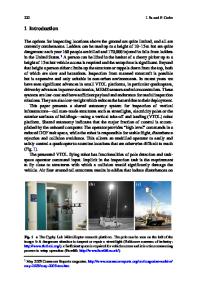
I. INTRODUCTION Non-memory semiconductors, which are used for input signals, data judgment, and output of results are mainly used for CPU, GPU, system on chip (SoC), and application chip (AP chip). They are used in the process of inspection which is called wafer probing inspection. The shape of the wafer probe is shown in Fig. 1 and the probes electrical and physical properties when it comes into contact with a water drop. Common drops range in size from 100 to 150 μm, and the probes in contact with them use fine components with diameters less than 100 μm. A typical probe card can consist of thousands and tens of thousands of probes, and various forms are used. The four main types of probes used in probe cards are the cantilever type [1–4], pogo type, vertical type [5–8], and MEMS type [9,10]. The cantilever type generates a large contact load and many scrubs on the drop during inspection. The spacing between drops is limited. The Pogo type has a large number of parts and high electrical contact stability, but the distance between bumps is limited due to the minimum thickness limit. The MEMS an excellent probe but has a disadvantage of high manufacturing cost. The vertical type has the advantage of high ∗ E-mail:
[email protected]
pISSN:0374-4884/eISSN:1976-8524
directivity, a bump array design, and constant contact load during wafer probing inspection [3,5–7]. The rapid development of the IT ind
Data Loading...